UV Organic Semiconductor Photoconductor with Low Dark Current at High Electric Field
- PDF / 3,489,696 Bytes
- 6 Pages / 612 x 792 pts (letter) Page_size
- 68 Downloads / 272 Views
UV Organic Semiconductor Photoconductor with Low Dark Current at High Electric Field Umar Shafique 1, Karim S. Karim 1,2 1
Department of Electrical and Computer Engineering, Nanotechnology Program, University of Waterloo, Waterloo, Ontario Canada 2
Center for Bioengineering and Biotechnology (CBB), University of Waterloo, Waterloo, Ontario Canada Email: [email protected]
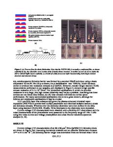
ABSTRACT Organic semiconductor technology paves the way to low cost lightweight, flexible, printable electronics circuits and sensors. A novel lateral multilayer organic semiconductor photosensor is fabricated using small molecule organic semiconductor. A specialized interface layer is introduced between the metal electrodes and the organic semiconductor layer. The interface layer material is a large band gap and low electronic conductivity material. The use of interface layer limits the charge injection from the electrodes to the organic semiconductor and overall improves the photosensor dark current performance with an additional advantage to apply high voltage for improved collection. This design has low dark current with high photo-to-dark current ratio and can be set to high bias mode of operation. Lateral interdigitated photodetector, with bottom contact Metal Semiconductor Metal (MSM) is fabricated consisting of interface layer and organic semiconductor bilayer. Small molecule organic semiconductor 3,4,9,10 perylenetetracarboxylic bisbenzimidazole (PTCBI) and CopperPhthalocyanine (CuPc) are used as the active bilayer, where as polyamide forms the interface layer. Current through the sensor is measured in both dark and in light (wavelength 400nm). The dark current density in a 1mm2 photosensor area with 5µm lateral electrode spacing at 10V/µm measured equal to 10-5mA/cm2 and a photocurrent density of 10-3 mA/cm2 under 0.3mW/cm2 incident optical power. The photo to dark current ratio is measured to be equal to ~103. This photosensor has an application in large area imaging for example portable lightweight detectors. Other applications of this sensor include indirect medial imaging and as a biosensor in UV Spectroscopy study of bacteria cultures. INTRODUCTION Organic semiconductor sensors and devices can be fabricated at low temperature, which allow the use of low cost plastic substrate. The use of plastic substrate give advantages such as mechanically flexible and light weight and portable [1]. Both the display, sensor industry and research groups have shown interest in organic semiconductor devices as a low cost alternative to the existing amorphous
silicon technologies. Most of the high efficient organic semiconductor photosensor reported today in literature, are vertical design (geometry) consisting of active organic semiconductor layers sandwiched in two conducting layer, typically metals, among which one needed to be transparent [2]. The other detector design is lateral photodetector designs. Lateral design consists of in plane electrode separated with an empty space that is the channel length. The lateral design can be either bo
Data Loading...


