Gate Bias Modulated Current Flow Analysis at Organic Semiconductor / Metal Interface for Developing High Performance Org
- PDF / 811,027 Bytes
- 6 Pages / 612 x 792 pts (letter) Page_size
- 88 Downloads / 279 Views
B9.32.1
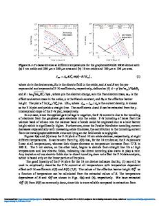
GATE BIAS MODULATED CURRENT FLOW ANALYSIS AT ORGANIC SEMICONDUCTOR / METAL INTERFACE FOR DEVELOPING HIGH PERFORMANCE ORGANIC FET Manabu Yoshida, Sei Uemura, Satoshi Hoshino, Takehito Kodzasa, and Toshihide Kamata, Photonics Research Institute, National Institute of Advanced Industrial Science and Technology, Central 5, 1-1-1 Higashi, Tsukuba, Ibaraki 305-8565, JAPAN ABSTRACT We have developed a current flow analysis system for Field Effect Transistors (FET) using a conductive cantilever of a probe microscope. Using this analysis system, nanoscale current images were observed on a pentacene active layer grown on a bottom electrode in ordinary FETs. When gold (Au) was employed as a bottom electrode, we found the special region around the electrode edge. The current flow hardly occurred in this region. On the other hand, using a conductive polymer (PEDOT) bottom electrode, such a region was not observed. From the detailed observation around the electrode edge, we concluded that the special region would be caused by diffusion of Au particles that evoked heterogeneous pentacene growth, and then the heterogeneity worked as a contact resistance. INTRODUCTION For long years, organic semiconductor/metal interfaces have attracted great attentions of many researchers, because the phenomena occurring at these interfaces strongly affect characteristics of electronic devices [1, 2]. For example, organic electroluminescence (EL) devices take advantage of the charge injections at the semiconductor/metal interface [3]. Similarly, it has been known that the organic FET performance is strongly governed by contact conditions at the organic semiconductor/metal interface under the gate bias as well as at the semiconductor/insulator interface [4]. Therefore, we should collect more information about semiconductor metal interfaces. For the investigation of the detailed interface condition, we have developed a current flow analysis system for directly observing the semiconductor/metal interface condition on a FET structure using a conductive cantilever of a probe microscope. This system allows us to obtain nanoscopic drain-source current mapping images under the gate bias. In this study, we have examined the electric field distribution around the source or drain electrode covered with several organic semiconductor layers under the gate bias. EXPERIMENTAL DETAILS Figure1 shows the cross-sectional illustration of our developed current flow system using SPI3800N probe station (Seiko Instruments inc.). Au-coated conductive cantilevers (elastic constant k = 0.14 N/m) were especially employed to take current images on device surfaces. A voltage source (Kepco ABC125-1DM) was connected to this system for applying gate voltages. Samples for obtaining current flow images were fabricated as following procedures. Heavily doped Si with thermally grown SiO2 (50nm) was employed as a substrate and a gate electrode. Substrates were carefully UV-ozone cleaned before the fabrication of FET devices. Pentacene was train-sublimated 5 times for purificati
Data Loading...