Radiation Damage Induced Transient Enhanced Diffusion of Dopants in Silicon
- PDF / 239,082 Bytes
- 5 Pages / 420.48 x 639 pts Page_size
- 23 Downloads / 426 Views
RADIATION DAMAGE INDUCED TRANSIENT ENHANCED DIFFUSION OF DOPANTS IN SILICON
R.ANGELUCCI, E.GABILLI, R.LOTTI, P.NEGRINI, M.SERVIDORI, S.SOLMI AND M.ANDERLE* CNR - Istituto LAMEL, Via Castagnoli, 1 - 40126 Bologna (Italy) * Divisione di Scienza dei Materiali, IRST - 38050 Povo, Trento (Italy)
ABSTRACT Transient enhanced diffusion is observed for P, As and Sb as a consequence of the recovery of the damage created by a silicon dose below the amorphization threshold. The phenomenon results more pronounced for low temperature furnace heating than after rapid thermal annealing and for those elements having a larger component of interstitialcy diffusion mechanism. A close correlation was found between the trends of the anomalous dopant diffusion and the implant damage evolution analyzed by X-ray diffraction. This evolution takes place via interstitial cluster dissolution.
INTRODUCTION The VLSI demand for shallow junctions has strongly lightened the postimplantation annealing treatments, thus emphasizing the effects of dopant transient anomalous diffusion. Most of the investigations, aimed to relate diffusion properties to damage evolution, were made with amorphizing dopant ion doses or with dopants immersed in surface homogeneous amorphous layers /1-4/. In these conditions marked enhanced diffusion was obsrved for P /1,2/, while minor effects occur for As /2,3/ and Sb /2,4/. This work reports the influence on P, As and Sb diffusion of the annealing induced evolution of lattice defects produced by low dose silicon ion implantation.
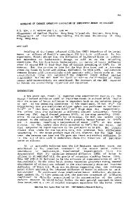
EXPERIMENTAL Anomalous dopant diffusion was checked by a suitable test structure /2,4/, which allows to compare in the same sample the junction depths in adjacent damaged and undamaged regions. The fabrication sequence of this structure is: (i) introduction of the dopant in surface layers about 0.1 um (shallow junctions) and 0.3 Iuum (deep junctions) thick: thermal predeI psition for P and ion implantation followed by high temperature annealing for As and Sb (in the last two cases, only wide and stable dislocation loops, if any, could be left); (ii) opening of alternating stripes of bare silicon by photolithography ý.4 loW temperature deposited oxide; (iii) selective implantation of ixl0 cm%, 100 keV silicon ions along the axis (axial channeling). The samples were then annealed by electron beam at 11000C for 10 sec or by conventional furnace heating at 700 and 750'C for increasing times. The differences in the junction depths AX. were measured by beveling and staining technique, whereas the dopant proiles were obtained by SIMS. The depth distributions of the lattice strain in the undoped, implanted specimens were determined by double crystal X-ray diffraction, according to the experimental and computing procedures reported previously /5/.
Mat. Res. Soc. Symp. Proc. Vol. 74. 11987 Materials Research Society
506
c) 140
10-3
10-4
a bb ,
C c
10-5 0
200
400
, 600
depth [nm] Fig.1
-
(C,)
Depth profiles of the strain component normal to sample surface after Si implantation and anneal
Data Loading...