Reactive Ion Etching of AlN, AlGaN, and GaN Using BCl 3
- PDF / 3,158,704 Bytes
- 6 Pages / 414.72 x 648 pts Page_size
- 108 Downloads / 331 Views
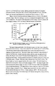
W. C. HUGHES, W. H. ROWLAND, JR., M. A. L. JOHNSON, J. W. COOK, JR., and J. F. SCHETZINA Department of Physics, North Carolina State University, Raleigh, NC 27695-8202 ABSTRACT The III-V nitrides are promising materials for use in UV-blue-green optoelectronics, high-temperature electronics, and negative-electron-affinity (NEA) electron emitter applications. In order to realize this potential, it is important to develop an etching technology for device fabrication. The stability of the III-V nitrides to harsh chemical environments makes most wet etching extremely difficult, so that dry etching alternatives are desirable. Recent experiments have shown that BCI 3 -based chemistries are effective for reactive ion etching of GaN and that KOH-based solutions may preferentially etch AIN from GaN. This paper reports on the use of BCI 3 for etching AIN and AIGaN in addition to GaN and the creation of structures such as mesas and lines. It also examines the potential use of potassium Hydroxide (KOH) as a wet etchant of the nitrides. AIN, AIGaN, and GaN films grown by either metal-organic chemical vapor deposition (MOCVD) or molecular beam epitaxy (MBE) were patterned with Ni in 250 I.m x 250 [tm squares and 5 Vm wide lines to create mesas and lines for typical light emitting diode (LED) or laser diode applications. Reactive ion etching was performed in a commercial reactor using BCI3 pressures ranging from 5 to 30 mTorr. Gas flow rates of 5 to 50 sccm and RF powers of 50 to 150 W were employed. High nitride etch rates of up to 730 A/min. were observed but lower etch rates were needed to avoid etching of the Ni mask. Smooth mesa surfaces and sidewalls were observed in scanning electron micrographs of the etched nitride structures. Mesas as small as 5 jim x 5 jIm were patterned and made in this way. Lines were also made in a similar manner as narrow as 5 jIm on GaN/AIN epilayers. Subsequent wet etching of these lines showed that KOH-based solutions such as AZ400K developer attack not only AIN but also GaN depending upon the quality of the film. Possibilities for using this wet etch as a defect etchant or selective etch of nitrides on SiC are discussed. INTRODUCTION The pursuit of short wavelength light-emitting devices based on wide band-gap semiconductors has been one of the most active areas of research in semiconductor physics over the past decade. After the initial successes of MBE-grown ZnSe-based II-VI semiconductors devices, GaN based materials have emerged at the forefront with Nichia Chemical developing commercial blue and green LEDs utilizing MOCVDgrown GaN and InGaN structures [1]. The commercial introduction of LEDs from III-V nitrides have led many researchers to consider new electronic and opto-electronic devices for which III-V nitrides may be well suited. In addition to their wide band-gaps, these materials also are quite chemically stable, allowing their use in other applications where resistance to harsh environments, high temperatures, or radiation is needed. There is also the possibility of using the negati
Data Loading...