Reliability Studies of Cu using Wafer Level Joule Heated Electromigration Test
- PDF / 1,071,260 Bytes
- 6 Pages / 417.6 x 639 pts Page_size
- 53 Downloads / 407 Views
ABSTRACT In this paper, we describe some of the results that we have obtained using Wafer Level Joule Heated Electromigration Test and Current Ramp Test. The results indicate that the Cu we tested is more resistive to open failure due to current ramp than Al-I%Si-0.5%Cu. The value of the activation energy for electromigration of Cu using fixed current under wafer level joule heated electromigration test is 0.59 eV. The activation energy due to the effect of temperature gradient failure mechanism is 0.82 eV.
INTRODUCTION As the demands on the performance and reliability in integrated circuits used in today's consumer products increases, manufacturers of ICs are looking for a replacement to the Al workhorse that has served as the interconnection of devices for the past few decades. Copper has been considered to be a candidate for the replacement of Al metallization used in integrated circuits because of its high resistance against electromigration and low resistivity value.
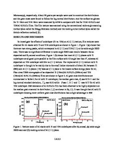
EXPERIMENT The test structure used for the wafer level joule heated electromigration test is a quasiNIST test structure. The schematic of the test structure is shown in Figure 2. The PVD-Cu is a single damascene structure with Ta as the diffusion.barrier. The thickness of Cu and Ta are 500 nm and 50 nm respectively. The Cu test structure is capped with 200 nm of silicon nitride and 300 nm of silicon dioxide. A cross-sectional FIB image of an 8 gm wide line is shown in Figure 1. Minimal dishing and erosion is observed in these lines.
Figure 1: Cross-section FIB of the tested structure: 8 micron wide damascene PVD-Cu line of thickness 500nm. The Diffusion Barrier used is Ta of 50 nrm. The cap layer is Silicon Nitride of 200 nm. The test structure is further passivated with silicon dioxide of thickness 300 nm. Image Scale: metal width shown in the FIB is 8 gm. 365 Mat. Res. Soc. Symp. Proc. Vol. 564 ©1999 Materials Research Society
Figure 2: Schematic diagram of a portion of Quasi-NIST test structure. A tapered lead into the test line is used. RESULTS AND DISCUSSION In the first experiment, a comparison of the resistance of Cu and AI-1%wtSi-0.5%Cu with and without underlayer Ti/TiN against current ramp test is conducted. A current density ramp rate of 0.357 mA/p4m 2 per 0.5 second starting at 10 mA is used as the current stress. Chuck temperature is maintained at 30 'C. The stress is applied until the line opens. The results in Figure 3 indicate that PVD Cu is more resistive to open failure because of higher current ramp than AI-1%Si-O.5%Cu. The conventional EM test [ 1] has illustrated that the electromigration lifetime of plated Cu is two orders of magnitude higher than that of the Ti/AI(Cu)/Ti test line. The results shown in Figure 3 indicate that damascene PVD-Cu can sustain a current density by a factor of two higher than that of AI(Cu) line before the line fails by open circuit, not drift as in a 2-level structure. In the comparison of damascene PVD-Cu and RIE CVD-Cu, the current ramp test seems to suggest that damascene PVD-Cu is better a
Data Loading...