Residual Ion Implantation Damage at Source/Drain Junctions of Excimer Laser Annealed Polycrystalline Silicon Thin Film T
- PDF / 1,280,752 Bytes
- 6 Pages / 612 x 792 pts (letter) Page_size
- 27 Downloads / 302 Views
Residual Ion Implantation Damage at Source/Drain Junctions of Excimer Laser Annealed Polycrystalline Silicon Thin Film Transistor Kee-Chan Park, Jae-Shin Kim, Woo-Jin Nam and Min-Koo Han School of Electrical Engineering, Seoul National University, Seoul, 151-742, KOREA. ABSTRACT Residual ion implantation damage at source/drain junctions of excimer laser annealed polycrystalline silicon (poly-Si) thin film transistor (TFT) was investigated by high-resolution transmission electron microscopy (HR-TEM). Cross-sectional TEM observation showed that XeCl excimer laser (λ=308 nm) energy decreased considerably at the source/drain junctions of top-gated poly-Si TFT due to laser beam diffraction at the gate electrode edges and that the silicon layer amorphized by ion implantation, was not completely annealed at the juncions. The HR-TEM observation showed severe lattice disorder at the junctions of poly-Si TFT. INTRODUCTION Low temperature polycrystalline silicon thin film transistors (LTPS-TFT) fabricated by excimer laser annealing (ELA) have attracted much attention for their possible application to driving circuitry of active-matrix liquid crystal displays and organic light emitting diode displays. However the electrical characteristics of LTPS-TFTs such as carrier mobility, subthreshold swing, threshold voltage, leakage current and stability are rather poor compared with those of the transistors fabricated on crystalline silicon wafers. It has been reported that the high defect density in the poly-Si channel layer and the poor electrical characteristics of the plasma-deposited gate insulator are responsible for these problems of LTPS-TFTs [1, 2]. Residual ion implantation damage at the source/drain junctions of LTPS-TFTs may also be one of the major causes of the large leakage current and the poor stability of LTPS-TFTs [3]. The source/drain region of LTPS-TFT is amorphized during the ion implantation for source/drain doping and recrystallized by ELA. However the source/drain junctions may not be fully annealed by ELA because the laser energy decreases considerably at the junctioins due to diffraction of laser beam at the gate electrode edges. As a result, a lot of crystalline defects remain at the junctions as shown in Fig. 1. It has been scarcely reported in detail about the generation mechanism and the structural property of the junction defects. In the present work, we report the decrease of laser energy due to diffraction at the gate electrode edge during ELA and the effect of laser energy density on the residual junction defects of LTPS-TFTs.
A7.6.1
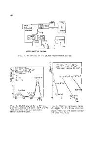
Figure 1. Cross-section of top-gated LTPS-TFT. Residual ion implantation damage remains at source/drain junctions.
EXPERIMENT In order to investigate the laser beam diffraction at the gate electrode edges, 700 Å thick amorphous silicon (a-Si) films were deposited on oxidized silicon wafer substrates by plasma enhanced chemical vapor deposition (PECVD) at 350 oC. Hydrogen in the PECVD a-Si films was removed by thermal annealing at 450 oC for 2 hours. 1000 Å thick tetrae
Data Loading...