Surface Roughening Transition in Si 1-x Ge x :H Thin Films
- PDF / 1,926,853 Bytes
- 6 Pages / 612 x 792 pts (letter) Page_size
- 91 Downloads / 328 Views
0910-A03-02
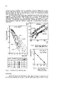
Surface Roughening Transition in Si1-xGex:H Thin Films Nikolas J. Podraza1, Christopher R. Wronski2, Mark W. Horn2, and Robert W. Collins1 1 Department of Physics and Astronomy, University of Toledo, Toledo, OH, 43606 2 Materials Research Institute, The Pennsylvania State University, University Park, PA, 16802 ABSTRACT In this study, the amorphous-phase roughening transition thickness has been determined as a function of process variables in plasma-enhanced chemical vapor deposition (PECVD) of hydrogenated amorphous silicon-germanium alloys (a-Si1-xGex:H). Among the process parameters varied include the H2-dilution gas flow ratio, the alloying flow ratio, the electrode configuration (anode vs. cathode), and the He-dilution ratio. One clear feature of this study is a maximum in the amorphous roughening transition thickness (and hence surface stability) at a H2dilution ratio just below the transition from amorphous to mixed-phase (amorphous+ microcrystalline) (a+µc) growth. A second feature for high Ge content films is a significant increase in the roughening transition thickness for cathode PECVD (with a self-bias of ~ −20 V) relative to anode PECVD. Additional features of interest involve suppression of the transition to (a+µc) for (i) alloying with Ge, (ii) biasing the substrate cathodic, and (iii) diluting the gas with He. The close correlation of high surface stability with enhanced short-range order and overall electronic performance has led to a simple model for the transition in terms of a competition between roughening due to the atomic size and smoothening due to precursor surface diffusion. It is proposed that diffusing precursors are immobilized by surface defects (or by other diffusing precursors), and the pre-existing (or resulting) defects are ultimately incorporated in the bulk. INTRODUCTION Extensive research on hydrogenated amorphous silicon (a-Si:H) thin films has shown that optimum device performance is correlated with the smoothest, most stable surfaces versus time during the PECVD process – in fact, less than a monolayer of roughening occurs throughout the deposition of optimum films as thick as 0.5 µm [1]. Such research requires smooth crystalline silicon substrates for high sensitivity to surface roughness as well as an in situ probe such as spectroscopic ellipsometry (SE) for real-time analysis. It has been also shown that when the PECVD conditions deviate from the optimum even slightly, e.g., by a reduction in the hydrogen dilution ratio or by an increase in plasma power from the minimum possible, then a roughening transition is observed in the a-Si:H growth regime [1]. This transition shifts to decreasing bulk layer thickness for films with increasingly deteriorated device properties. As a result, the thickness at which the roughening transition (denoted a → a) occurs has been entered into deposition phase diagrams, relevant for c-Si substrates, that provide insights into the device quality of a-Si:H and how it varies with deposition parameters. In the present study, the roughen
Data Loading...