Scanning Tunneling Microscopy Studies of GaAs Heteroepitaxial Growth on Si
- PDF / 2,912,248 Bytes
- 12 Pages / 420.48 x 639 pts Page_size
- 73 Downloads / 361 Views
SCANNING TUNNELING MICROSCOPY STUDIES OF GaAs HETEROEPITAXIAL GROWTH ON Si D. K.BIEGELSEN, R. D. BRINGANS, J. E.NORTHRUP, AND L.E. SWARTZ Xerox Palo Alto Research Center, 3333 Coyote Hill Road, Palo Alto, CA 94304
ABSTRACT We discuss the benefits and limitations of scanning tunneling microscopy (STM) for use in studies of the early stages of heteroepitaxy. We describe a system merging in vacuo an MBE, STM, XPS, LEED, etc. We present results for the initial stages of GaAs growth on vicinal Si(100), including As termination, Ga capping and subsequent 2D and 3D competition.
INTRODUCTION The successful heteroepitaxial growth of compound semiconductors on Si could obviously form the basis for novel, monolithically integrated optoelectronic systems. In all material couples studied to date, for example, GaAs/Si, GaP/Si, GexSil-x/Si, SiC/Si, etc., a long sequence of stages can be delineated before one attains a steady state, uniform, essentially homoepitaxial growth. These stages may include monolayer coverage, island nucleation, growth and coalescence, introduction of dislocations, introduction and perhaps annihilation of antiphase domains, etc. It is clearly desirable to obtain device quality material with a minimum transition layer thickness. To achieve this (with understanding), one would like to observe the stages of nucleation and growth. In this paper we describe the use of scanning tunneling microscopy (STM) to address some of these issues.
SCANNING TUNNELING MICROSCOPY Scanning tunneling microscopy has proved itself as a unique means for imaging local, real-space structures of semiconductor surfaces. Studies of Si(100) homoepitaxial surfaces, for instance, have directly demonstrated anisotropic nucleation.[1,21 It has also been inferred that surface roughening at the growth temperatures used is blocked by the 900 rotation of island anisotropy from layer to layer - i.e., long nuclei must fit onto narrow terraces.[1 I Other notable examples of homoepitaxy are the various reconstructions of the GaAs(100) [3,41, GaAs(111) [51 and GaAs(111) [6] surfaces. In this paper we will describe the application of STM to heteroepitaxy, specifically GaAs on vicinal Si(100). We will address some of the strengths and weaknesses of STM as a tool for in situ studies. Ideally, STM would provide real Mat. Res. Soc. Symp. Proc. Vol. 198. @1990 Materials Research Society
360
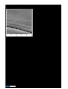
time atomic images of a section of the substrate during growth. Although not impossible, the presence of the STM in a molecular beam epitaxy (MBE) system, for example, would drastically alter the deposition conditions from those for optimal MBE. Specifically, the proximity of the tip to the surface would limit the approach angle of the beams to neartangential incidence, as shown in Fig. 1. (A tunnel gap of 10 A and a limiting radius of curvature of 40 A, say, would result in an acceptance angle 0 = 370.) The MBE environment would also be detrimental to the operation of the STM. Any component of the beam fluxes sticking to the tip would change the tunneling drast
Data Loading...