Scanning Tunneling Microscopy of Nanoindentations
- PDF / 2,400,652 Bytes
- 4 Pages / 420.48 x 639 pts Page_size
- 18 Downloads / 417 Views
SCANNING TUNNELING MICROSCOPY OF NANOINDENTATIONS MARTIN R. CASTELL* AND TIMOTHY P. WEIHSI *Cavendish Laboratory, Madingley Road, Cambridge CB3 OHE, UK. tDepartment of Materials, Parks Road, Oxford OX I 3PH, UK.
ABSTRACT A scanning tunneling microscopy (STM) study of low load indentations into Si, GaAs and Au is presented. Compared with standard micrographs obtained through optical microscopy and scanning electron microscopy, the STM images show greatly improved resolution in and around the indentation. The effects of relaxation and pile-up may be observed through contour plots which show inward bowing of the indentation faces in Si.
INTRODUCTION With the advent of STM it has become possible to study surface topography on the atomic scale. Using suitable imaging software, one can utilize this resolution to produce contour plots of very small areas. This capability can prove very useful when examining the geometry of small indentations [1]. In this paper we describe STM images and STM contour plots of small indentations into Si, GaAs and Au. Subsequent analysis reveals information regarding the modes of deformation during the indentations and the final shape of the indentation areas after unloading.
EXPERIMENTAL PROCEDURES All indentations were made using a Nanoindenter (manufactured by Nano Instruments, Inc.) and a Berkovich diamond tip. The tip is a three-sided pyramid ground to the same depth to area ratio as a Vickers pyramid. Indentations were performed at room temperature using a constant loading rate that scaled with the maximum load applied during a test. The load applied to the tip and the displacement of the tip were recorded continuously. Si samples were cut from a polished n-type, Sb doped (100) wafer with a carrier density of nc= 2 .9 x 1018 cm- 3 and patterned with an indentation array ranging in loads from 0.4mN to 25mN. Subsequent STM imaging required the removal of the native oxide layer and Hpassivation of the surface which was achieved using the UV/HF treatment described by 7 Takahagi et al [2]. GaAs samples were cut from a polished (100) p-type wafer (nc-101 cm3) and subsequently indented with a range of loads from 0.4mN to 40mN. A 1251.tm thick Au film was mounted on a resin support, polished mechanically and then coated with an additional layer of evaporated Au in the hope of smoothing the polished surface. This sample was then indented in a load range extending up to 100rmN. During typical STM operation we used etched Pt/Ir tips with a tip-sample bias of +1. IV and a tunneling current of 0.1 nA for the semiconductors and a +40mV bias and a I nA tunneling current when scanning the Au sample. Periodically, these parameters and other scanning conditions were changed to determine their effect on image quality. Our STM calibration procedure has been described elsewhere [1]. To improve the imaging conditions for the GaAs indentations, it was necessary to coat the indented sample with a 6nm film of Au.
Mat. Res. Soc. Symp. Proc. Vol. 239. (c)1992 Materials Research Society
368
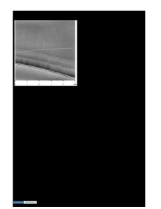
RESULTS Fig. la
Data Loading...