Schottky I-V Characteristics of Au/Ni/GaN/SiN x nanonework/sapphire structures
- PDF / 103,369 Bytes
- 4 Pages / 612 x 792 pts (letter) Page_size
- 8 Downloads / 276 Views
0955-I15-34
Au/Ni/GaN/SiNx Nanonework/sapphire Schottky I-V Characteristics Jinqiao Xie1, Yi Fu1, Hadis Morkoc1, Jinqiao xie2, and Jinqiao xie2 1 Department of electrical engineering, Virginia Commonwealth University, Richmond, VA, 23284 2 Virginia Commonwealth University, Richmond, VA, 23284 Schottky I-V Characteristics of Au/Ni/GaN/SiNx nanonework/sapphire structures Jinqiao Xie, Yi Fu and Hadis Morkoç Department of Electrical and Computer Engineering, Virginia Commonwealth University, Richmond, VA 23284, USA
ABSTRACT GaN epilayers were grown by metalorganic chemical vapor deposition using in situ SiNx nano-network. Crystalline quality of epilayers was characterized by X-ray rocking curve scans, and the full width at hall maximum values for (002) and (102) diffractions were improved from 252 arc sec and 405 arc sec, respectively, in control samples to 216 arc sec and 196 arc sec when SiNx was used. Ni/Au Schottky diodes (SDs) were fabricated and the SD performance was found to be critically dependent on the SiNx coverage which is consistent with the trends of XRD and photoluminescence data. A 1.13eV barrier height was achieved when 5 min SiNx nano-network was used compared to 0.78 eV for reference sample. Furthermore, the breakdown voltage was also improved from 76 V to 250V. INTRODUCTION III-Nitrides based devices perform increasingly well in light-emitting diodes (LEDs), laser diodes (LDs), ultraviolet detectors, and field effect transistors1. To improve the device performance and reliability further, a variety of methods which mainly rely on epitaxial lateral overgrowth (ELO)2 have been developed. One disadvantage of ELO is that it requires ex situ photolithographic steps. Recently, techniques based on micro scale ELO using in situ deposited SiNx nano-network3, ex situ TiNx network4, and porous SiC5 have been used with promising results. In this paper, we report on the effect of SiNx interlay deposition conditions on the electrical properties of GaN grown on 2-inch sapphire substrates, as well as structural and optical properties. EXPERIMENT GaN epilayers were grown in a vertical low pressure metal organic chemical vapor deposition (MOCVD) system. After a low temperature (LT) GaN nucleation layer, ~2 µm GaN was deposited followed by in-situ SiNx deposition and 4 µm GaN film without interruption. All samples were unintentionally doped, and the only difference between samples was the SiNx deposition time which varied from 0, 3, 4, 4.5, 5 to 5.2 minutes.
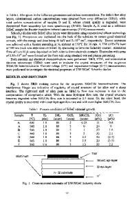
Planar Schottky diodes (SDs) were fabricated using standard photolithography. Ti/Al/Ti/Au (30/100/30/100 nm) ohmic contacts were deposited by e-beam and thermal evaporation, followed by a 60 second rapid thermal annealing at 900°C in nitrogen ambient. 200 µm-diameter Ni/Au (30/120 nm) SDs were deposited by e-beam evaporation. The separation between SDs and ohmic contacts was 50µm. The current–voltage (I–V) was measured by using a Keithly 4200 parameter analyzer. RESULTS and DISCUSSIONS Typical room temperature I-V characteristics of Ni/Au SDs are plotted in Fi
Data Loading...


