Si Nanocrystals by Metal Induced Growth using Different Catalyzing Metals
- PDF / 1,585,485 Bytes
- 6 Pages / 612 x 792 pts (letter) Page_size
- 19 Downloads / 283 Views
F8.3.1
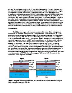
SI NANOCRYSTALS BY METAL INDUCED GROWTH USING DIFFERENT CATALYZING METALS Chunhai Ji and Wayne A. Anderson University at Buffalo, The State University of New York, Dept of Electrical Engineering, Buffalo, NY. ABSTRACT A comparative study of nanocrystalline silicon thin films grown on 25 nm thick catalyzing metals by dc magnetron sputtering from a highly doped Si target has been performed. In our previous study, the growth of Si was catalyzed by the silicide reactant from sputtered Si and Ni. These new experiments compared the effect of two types of catalyzing metals, Ni and Co. The structural and electrical characteristics of nano-Si were examined by scanning electron microscopy (SEM), cross-section SEM (XSEM), transmission electron microscopy (TEM), fourpoint-probe measurement and Schottky contact I-V measurement. The SEM and XSEM revealed that, for both catalyzing metals, the nano-Si thin films have columnar nano-grains with length of 500 nm in the vertical direction. However, the diameter of grains strongly depends on the catalyzing metals. For Co, the nano-Si grains had a typical diameter of 30 nm, while for Ni, the grains were much larger. TEM analysis showed that this difference in grain size begins at the initial growth stage. In the later-on growth, the Si grains mainly grow in a vertical direction instead of a lateral direction. This implies that the dimensions of Si nanostructures are strongly determined by the initially formed metal silicide nanoparticles. The current-voltage curve of a fabricated Al Schottky diode on P-type Co catalyzed nano-Si exhibited good rectifying characteristics. The dopant has been naturally synthesized in the Si nanocrystals during the growth of nano-Si by using a doped sputtering target. The above measured electrical properties show that metal induced grown nanocrystalline Si is applicable to various electronic and photonic devices. INTRODUCTION In the process of metal induced growth (MIG), a thin metal layer was deposited on the substrate by thermal evaporation. At increased temperature, the sputtered Si reacted with the metal to form a thin silicide layer which has an extremely small lattice mismatch with Si. Then, the deposited Si epitaxially grows into nc-Si or µc-Si on the metal silicide. By the MIG process, the nc-Si growth temperature can be decreased to as low as 500 °C. This may reduce the fabrication cost and permit the use of cheap foreign substrates e.g. glass for certain applications. So far, only a few papers concern the heteroexpitaxal growth of nc-Si films from metal silicide which forms during or before the nc-Si film deposition [1-3]. In previous studies, we have described growth mechanisms of nc-Si films by the MIG method in the Si/NiSi2 system with 0.4% lattice mismatch [4,5]. Ni is not the only metal of choice and was used here only as an initial step in studying the MIG phenomenon. This paper reports and discusses the Si nanostructure differences between the Si/NiSi2 and the Si/CoSi2 system. The Co system offers some advantages which are described
Data Loading...