Solar Cells on Foreign Substrates using Poly-Si Thin Films by Metal Induced Growth
- PDF / 104,380 Bytes
- 6 Pages / 612 x 792 pts (letter) Page_size
- 21 Downloads / 324 Views
A4.21.1
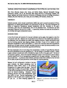
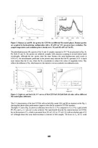
SOLAR CELLS ON FOREIGN SUBSTRATES USING POLY-SI THIN FILMS BY METAL INDUCED GROWTH Chunhai Ji and Wayne A. Anderson Department of Electrical Engineering, University at Buffalo, Amherst, NY14260 Abstract The poly-Si film was deposited by using the metal-induced growth (MIG) method on tungsten substrates. By making Au/n-Si Schottky photo-diodes, doping density effect was studied by using three different doping level Si sputtering targets. Increasing the Si target resistivities from 0.02Ω-cm to 50Ω-cm, open-circuit-voltage (Voc) decreased from 0.22V to 0.14V while short-circuit-current density (Jsc) increased from 1.55mA/cm2 to 2.42mA/cm2. C-V results revealed a high charge density in the device, which may be due to the oxygen thermal donor effects. Using an oxygen filter for the sputtering gas effectively reduced the charge densities and increased the Jsc value. The p/n junction solar cells were fabricated by using ion implantation at 1013~1014cm-2 dose and 100~200keV. The cells with wider emitter layer by double-ion implantation gave higher Jsc and Voc values. Passivation of the Si film by using hydrogenation improved the Jsc, Voc and spectral response of the solar cells. Introduction Thin film Si is an important material for low-cost solar energy conversion. Comparing with a-Si, poly-Si has higher carrier mobilities and less degrading of film properties under illumination [1]. The grain size of poly-Si is expected to be large in order to reduce the carrier recombination at grain boundaries [2]. To achieve the large grains in the Si film, secondary crystallization or grain growth is usually applied to asdeposited a-Si or small grain Si films. Direct-deposition of large grain Si is desired due to process simplicity. However, the higher temperature is always needed for grain growth and producing high quality films. In order to use a low-cost glass substrate, it is necessary to grow the poly-Si film at temperatures lower than the glass softening point, about 600°C. Metal-induced growth (MIG) has been proposed and studied due to potentially reduced process cost and decrease in the thermal budget [3,4]. In the MIG process, the Ni or Co seed layers with a thickness of 25~50nm were evaporated on tungsten (W) substrates. At the elevated temperature (525°C~600°C), the sputter-deposited Si reacts with these two metals to form NiSi2 or CoSi2. Thereafter, the Si film is in polycrystalline form by heteroepitaxially growing on the NiSi2 or CoSi2 layer due to the same lattice structure between Si and silicide but with extremely small lattice mismatch (1.2% for CoSi2 and 0.4% for NiSi2). The growth mechanisms have been studied intensively and a heteroepitaxial model was used to explain the growth of poly-Si films [4]. The similar epitaxial growth of crystalline Si film was studied by other groups in recent years which shows the increasing interest of this area [5,6]. In addition, a twostep sputtering process has been developed in order to produce device quality Si films with enough thickness (e.g. 5 µm) for light absorption
Data Loading...