SiC-based 1D Nanostructures
- PDF / 1,924,739 Bytes
- 6 Pages / 432 x 648 pts Page_size
- 82 Downloads / 336 Views
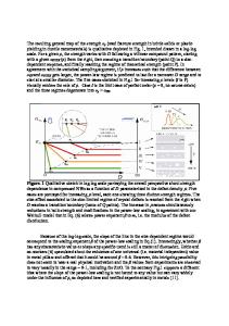
SiC-based 1D Nanostructures Maelig Ollivier1,2,3*, Laurence Latu-Romain1*, Mickaël Martin1, Arnaud Mantoux3, Edwige Bano2 1
Laboratoire des Technologies de la Microélectronique, CNRS UMR 5129, 17, rue des martyrs, 38054 Grenoble cedex 9, France 2 IMEP-LAHC Grenoble INP - Minatec: 3, rue Parvis Louis Néel - BP 257 - F38016 Grenoble Cedex 1, France 3 SIMaP, Grenoble-INP, CNRS, UJF, 1130 rue de la piscine, BP 75, 38402 Saint Martin d’Hères, France ABSTRACT Thanks to an original approach based on the carburization of silicon nanowires, silicon carbide-based one dimensional nanostructures – SiC nanotubes, Si-SiC core-shell nanowires and SiC nanowires – have been synthesized. The original process, which relies on controlling the out-diffusion of Si atoms through SiC, can be monitored by the temperature, the pressure and the time of carburization. These SiC-based 1D nanostructures have been characterized by SEM, FIBSEM and TEM microscopies and also Raman spectroscopy. Bio-nano-sensors, nano-FieldEffect-Transistors (nano-FETs) or gas sensors may be some applications for these nanostructures. INTRODUCTION In recent years, elaboration of one-dimensional (1D) nano-objects has been intensely studied because of their remarkable physical, optical and electrical properties, as well as a high surface to volume (S/V) ratio. Thanks to these properties, great potential applications of these structures in nanoelectronics and nano-biotechnology are conceivable [1]. On the other hand, silicon carbide, especially in the cubic phase, has remarkable electrical and physical properties such as high breakdown field, high band gap, high thermal conductivity and biocompatibility [2, 3]. Combining in the same object 1D-nanostructures properties and SiC properties, SiC-based 1D nanostructures are very interesting for specific applications such as bio-nano-sensors [4, 5], nano-Field-Effect-Transistors (nano-FETs) [6, 7] or gas sensors [8] for example. Important work on SiC nanostructures growth has been already achieved and numerous growth methods can be reported. The growth of SiC nanowires (NWs) can be achieved either by silicidation of carbon nanotubes [9, 10, 11], or by carbothermal reduction of sol–gel derived silica xerogels containing carbon nanoparticles [12], or by the well-known vapor-liquid-solid mechanism and affiliated methods such as vapor-solid growth [13, 14]. On the other hand, SiC nanotubes have been less studied and very few growth methods have been reported. This growth of SiC-NTs is usually done by the silicidation of carbon NTs, according to the shape memory synthesis [16, 17]. However, for all these SiC-based 1D nanostructures, there is some challenges before producing them with a sufficient quality. Indeed all the above methods lead to the same result: SiC cristallinity is rather mediocre, with a high density of structural defects such as twins and stacking faults [15]. Furthermore the doping level of SiC in the 1D-nanostructures is still not monitored.
23
In this paper an original process for the synthesis of SiC-based
Data Loading...