Silicide Formation using Laser and Electron Beams
- PDF / 3,260,222 Bytes
- 13 Pages / 415.8 x 637.2 pts Page_size
- 9 Downloads / 404 Views
511
Processing
SILICIDE FORMATION USING LASER AND ELECTRON BEAMS
T. W. SIGMON Stanford Electronics Laboratories,
Stanford,
California
94305
ABSTRACT The reaction of thin metal films with single crystal or amorphous silicon to form silicide compounds has been successfully undertaken using both scanned-cw and pulsed beam processing. Similar to the case for beam annealing of ion-implanted semiconductors, both the basic mechanisms and the experimental results are found to depend on whether pulsed or scanned beams are used to promote the reactions. For both cases the experimental results are often found to differ sharply from those obtained with standard furnace processing. For the pulsed beam reaction, melting and rapid resolidification occurs in the metal silicon films. The principal result is that the reacted film is frozen in a mixed phase compound which can consist of several silicide compounds including silicon and metal precipitation. Compositions inaccessible by conventional furnace annealing can also be formed by this process. In contrast to the pulsed beam results, scanned-cw beam processing of metal silicon films is found to result in the formation of large area uniform silicide phases with essentially no silicon or metal precipitation. These films are generally found to be homogeneous with well defined silicon/silicide interfaces.
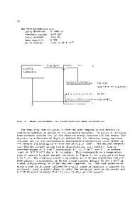
INTRODUCTION The reaction of thin metal films with both single crystal and amorphous silicon to form silicide compounds is an area that has been receiving considerable attention. The interest in this area arises from the fact that future trends in silicon integrated circuit technology, particularly the push towards higher device packing density and decreased dimensions, will require low resistance, thin film materials with high temperature properties that are compatible with other silicon processing operations. Such films will find important application as gates for MOS transistors, device interconnects and ohmic contacts [1-3]. Within the last two years, the use of laser, electron and ion beams to react metal/silicon films has also been actively investigated [4-11]. New and unique features provided by these forms of processing include shorter reaction times, localized heat treatment and rapid heating and cooling rates. As in the case of beam annealing of ion implanted semiconductors, both the basic mechanisms and the experimental results depend on whether pulsed or scanned-cw beams are used to promote the reactions. For both cases experimental results are found in many cases to differ sharply from those obtained with standard furnace processing. In Figure 1, from Lau, et al. [12] we illustrate the various approaches that are presently available for the formation of silicide compounds. Since excellent reviews of the use of both thermal [13] and ion beam mixing [14] to form silicides are presented elsewhere, we will concentrate primarily upon the use
512 of pulsed lasers and electron beams, and scanned-cw in the formation of the silicide compounds.
lasers and electron bea
Data Loading...