Silicon Interposer Reliability Optimization through Process-Oriented Stress Modeling
- PDF / 702,443 Bytes
- 6 Pages / 612 x 792 pts (letter) Page_size
- 82 Downloads / 327 Views
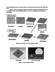
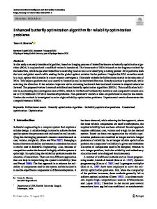
Silicon Interposer Reliability Optimization through Process-Oriented Stress Modeling Sri Ramakanth Kappaganthu1, Aditya Karmarkar1 and Xiaopeng Xu2 1 Synopsys (India) Private Limited, Hyderabad, Andhra Pradesh 500032, India 2 Synopsys, Inc. 700 East Middlefield Road, Mountain View, CA 94043, U.S.A. ABSTRACT A process-oriented stress modeling methodology is developed to investigate the stress evolution during the silicon interposer packaging process. An FEM based 3D TCAD simulator is used to perform the process steps to construct the silicon interposer stack in sequential order. These steps include TSV fabrication for passive silicon interposer, micro-bumping and reflow process for integrating active dies and passive interposer, C4-bumping and reflow for interposer BT-substrate stacking, and epoxy mold curing for interposer encapsulation. Stress simulations are carried out for each process step to obtain accurate stress evolution history. To resolve micron features within millimeter structures, the modeling strategy employs symmetry conditions, and equivalent materials for regions away from structure features of interest. The detailed structure includes 3x3 arrays of microbumps, TSV arrays, and C4-bumps with multiple material layers at the stack corner. Important design parameters include interposer thickness and edge clearance. For different silicon interposer configurations critical stresses in the outmost microbump and C4-bump are analyzed and compared. The reliability implications are discussed. INTRODUCTION Advanced electronic packaging needs to meet the requirements of reducing data latency, enhanced power management, continuously growing I/O pin density and constricted package footprint. Silicon interposer, with array of through-silicon-vias (TSVs), reduces the mismatch in the coefficient of thermal expansion (CTE) with respect to the die, improves thermal conduction at the die interface and provides very short interconnect length and large I/O density. Multiple dies with different functions, such as logic, memory and analog, are laterally integrated on a single interposer with lead-free solder microbumps. Multilevel damascene copper wires connect different dies horizontally in the interposer with dense connectivity. TSVs provide the pathways through the interposer. The die-interposer stack is attached to a substrate through an array of controlled collapse chip connection (C4) bumps. This hybrid integration with microbumps, TSVs, and C4-bumps serving as secondary interconnects is often called 2.5D IC. It is a promising packaging technique that provides high integration densities, heterogeneous integration and improved IC reliability. The packaging process for the silicon interposer stack involves several thermal cycles for the intermediate structures. It introduces thermal mismatch stresses at different steps due to the large difference in thermal expansion coefficients of the constituent materials. These residual stresses may lead to yield loss and reliability concerns. Interactions between the constituent st
Data Loading...