Silicon Thin Film Deposition on Nano-Structured ZnO Substrates
- PDF / 3,192,166 Bytes
- 5 Pages / 595 x 842 pts (A4) Page_size
- 65 Downloads / 360 Views
Silicon Thin Film Deposition on Nano-Structured ZnO Substrates R. Könenkamp, V. Chu*, J. Conde# and L. Dloczik Hahn-Meitner Institut Berlin, Glienicker Str. 100, 14109 Berlin, Germany # Dept. of Materials Engineering, Instituto Superior Tecnico, Av. Rovisco Pais, 1049-001 Lisbon, Portugal * Instituto de Engenharia de Sistemas e Computadores, Rua Alves Redol 9, 1000-029 Lisbon
ABSTRACT Amorphous and micro-crystalline Si films have been deposited by the hot-wire technique on deeply structured columnar ZnO films. It is found that nearly perfect conformal deposition occurs for amorphous films, similar to what was previously found for rf-plasma deposited films. Micro-crystalline films deposited by the hot wire technique are less conformal since deposition occurs preferentially on protruding features of the substrate, while films deposited by rf-plasma CVD exhibit high conformality.
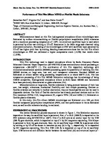
INTRODUCTION Semiconductor deposition on highly structured substrates becomes increasingly important as requirements for electronic circuits in thin film applications become more complex. Highly structured substrates are also of interest for photoelectrical, optoelectronic, and photonic devices, where light scattering, guiding and localization are to be exploited. We have recently investigated thin film deposition on several types of deeply structured substrate (1-3). Columnar ZnO films, as shown in Fig. 1, consisting of free-standing vertically aligned crystallites with a typical length of 2 µm, diameters of 200 nm, and a spacing of 500 nm were used as substrates for amorphous Si films grown by plasma assisted CVD (2). Interest in these ZnO/a-Si:H thin film structures stems from the potential to prepare an extremely-thinabsorber-type solar cell (3), based on thin film Si. In such a device the highly structured ZnO layer will achieve efficient coupling of the incoming light into the absorber, and, at the same time, will reduce the transport path for photogenerated carriers. Here we extended our previous investigation to the amorphous and micro-crystalline films grown by the hot wire technique.
Figure 1: Uncoated mono-crystalline ZnO columns grown by electro-deposition on SnO2 substrate.
A24.5.1
EXPERIMENTAL DETAILS Undoped a-Si:H films were deposited in a hot-wire CVD reactor at substrate temperatures of 250° C using 100 % SiH4 at a flux of ~20 sccm at a wire temperature of 2500° C, and pressure of 20 mTorr. Micro-crystalline films were deposited in the same reactor using 10 % SiH4 in H2 and otherwise similar conditions (4). The ZnO columns were prepared from aqueous solutions of 10-3 M ZnCl2 and 0.1 M KCl at 80 o C on micro-crystalline SnO2 substrates using a standard three-electrode reactor (2,5). The deposition potential was -1 V vs. standard calomel electrode potential. Fig. 1 shows the columnar ZnO film in the as-grown state. It is noted that the columns usually have hexagonal cross-section and plane crystalline faces. Typically the columns are 2 µm long, the distribution is random with typical inter-column distances of 500 nm; the
Data Loading...