Specific features of kinetics of molecular beam epitaxy of compounds in the GaN-AlN system
- PDF / 272,933 Bytes
- 6 Pages / 612 x 792 pts (letter) Page_size
- 20 Downloads / 378 Views
STRUCTURE AND NONELECTRONIC PROPERTIES OF SEMICONDUCTORS
Specific Features of Kinetics of Molecular Beam Epitaxy of Compounds in the GaN–AlN System A. N. Alekseev, A. É. Byrnaz, D. M. Krasovitsky, M. V. Pavlenko, S. I. Petrov^, Yu. V. Pogorel’sky, I. A. Sokolov, M. A. Sokolov, M. V. Stepanov, A. P. Shkurko, and V. P. Chalyi ZAO Svetlana-ROST, p/o box 29, St. Petersburg, 194156 Russia ^e-mail: [email protected] Submitted December 28, 2006; accepted for publication January 15, 2007
Abstract—The effect of growth conditions (V/III ratio, substrate temperature) on the properties of materials in AlN–GaN systems is discussed. A concept of the growth of the AlN/AlGaN/GaN multilayer heterostructure, which provides the improvement of crystal quality and surface morphology of the layers, is suggested and realized. The improvement of the properties of GaN in the AlN/AlGaN/GaN/AlGaN multilayer heterostructure is confirmed by a considerable increase in electron mobility in the two-dimensional electron gas formed at the upper heterointerface GaN/Al0.3Ga0.7N. PACS numbers: 71.55.Eq, 74.78.Fk, 81.15.-z, 81.16.-c DOI: 10.1134/S1063782607090011
1. INTRODUCTION Due to their unique properties, nitrides of Group III metals (III–N) are very promising for the fabrication of various semiconductor devices. The band gap of these direct-gap semiconductors overlaps the entire visible wavelength range and a considerable part of the ultraviolet region, which provides the basis for the fabrication of optoelectronic devices in the mentioned spectral regions [1]. Their high thermal and radiation stability, high breakdown fields, and clearly pronounced polarization effects make these materials attractive for hightemperature high-current electronics [2]. However, the technological difficulties in obtaining nitrides of Group-III metals for a long time hampered the practical realization of the advantages of these materials, and only in the last decade has significant progress been made in the technology of growing nitrides and fabrication of devices on their basis. One of the most important technological problems is the absence of sufficiently inexpensive substrates for homoepitaxial growth. Heteroepitaxy of nitrides on substrates made of materials which are to a certain extent mismatched by the lattice parameters and thermal expansion coefficients, despite application of special procedures at the initial growth steps, leads to a rather high dislocation density, which complicates the problem of obtaining device heterostructures. The main methods of growing device heterostructures from nitrides of Group-III metals are metal-organic chemical vapor deposition (MOCVD) and molecular beam epitaxy (MBE). In the MOCVD-grown layers, the dislocation density is on average lower by 1–1.5 orders of magnitude compared to the MBE-grown layers. The
decrease in the dislocation density is most probably associated with the higher substrate temperatures which are characteristic of MOCVD. This circumstance manifests itself in the better coalescence of the nuclei’s block
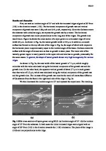
Data Loading...