Strain Measurements in a Thermally-Cycled Flip-Chip PBGA Solderball
- PDF / 1,462,095 Bytes
- 6 Pages / 417.6 x 639 pts Page_size
- 79 Downloads / 308 Views
at. Res. Soc. Symp. Proc. Vol. 563 ©1999 Materials Research Society
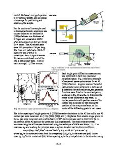
data reported are for a flip-chip PBGA package, at the solderball scale. In this study, electron-beam (e-beam) moireg,9 was used to study deformations in a flipchip PBGA package containing eutectic solderballs and fused Si0 2 underfill during a thermal cycle between -55 and 125 'C. I observed the thermomechanical deformations at different locations across the cross section of the package. U-field and v-field displacement data were acquired at each location at the temperature extremes and at room temperature. EXPERIMENT NIST received samples of flip chip on a plastic ball grid array substrate (Figure 1) from a major U.S. manufacturer. The specimen reported in this paper was cross sectioned, polished, and instrumented with crossed-line gratings at preselected locations. The specimen was cross sectioned along the long dimension of the chip and the solderballs observed were on the outermost row. Please see references 8 and 9 for details on the sample preparation and lithographic process. Each grating is approximately 450 x 450 gtm in area and has a pitch of 450 nm. A typical crossed-line grating is shown in Figure 2. Two locations are discussed here. Figure 3 shows the approximate locations of the two patterns on a diagram of the cross section of a flipchip package. The thermal loading test was conducted in the scanning electron microscope (SEM) on a commercially available heating/cooling stage with a temperature range of -196 to 400 'C. The specimen was thermally cycled between -55 and 125 'C. The 480 raster lines per field of view, produced by the SEM used in this study, interfered with the 1023 lines instrumented on the surface of the patterned area to produce moir6. As the raster encounters the raised edges of the grating line a strong signal is produced (bright fringe). If the raster falls in the trench of the exposed radiation-sensitive resist, then little signal is produced and a dark fringe results. The desired temperature is attained through balancing the liquid-nitrogen-cooled gas with a resistive heater. The grating is observed and when there is less movement than 1/ line/min, thermal equilibrium is considered to be reached and an image collected. With this technique, fringes known as carrier fringes are usually present in the initial noload condition images. This carrier-fringe field must be subtracted from the thermally-loaded fringe fields to obtain the change in the number of fringes in the fringe field due to the thermal load. Each change of one fringe is the indication that 450 nm of displacement has occurred; an increase of one fringe is due to 450 nm of expansion and a decrease of one fringe is due to 450 nm of contraction.
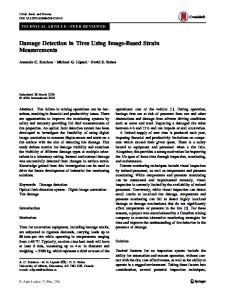
Figure 1. Image of flip-chip PBGA specimen as received from the manufacturer,
Figure 2. Example of an electron-beam moire crossed-line grating.
10
V Y' Pattern #3 t II
Pattern #1•
Solderball "i..
Sic hip Underfill JCB U, X
Figure 3. Cross section of flip-chip PBGA with approximate locations of the pattern
Data Loading...