Stress and Microstructure Evolution during the Deposition and Crystallization of DCMagnetron Sputter Deposited Amorphous
- PDF / 160,116 Bytes
- 5 Pages / 612 x 792 pts (letter) Page_size
- 74 Downloads / 303 Views
Stress and Microstructure Evolution during the Deposition and Crystallization of DCMagnetron Sputter Deposited Amorphous ITO
Hyo-Young Yeom, Courtney Lanier, Eric Chason, and David C. Paine Brown University, Division of Engineering, Box D Providence, RI 02910
ABSTRACT
The deposition of ITO onto glass substrates at room temperature results in a metastable amorphous phase that undergoes crystallization at remarkably low homologous temperatures (T/Tm90% at λ=550 nm) electrode material deposited onto heat sensitive polymer substrates. At these low temperatures (max circa 100°C) it is well known[5] that as-deposited films less than 90 nm thick are fully amorphous while thicker films may be fully or partially amorphous. Optimization of deposition parameters such as: deposition rate, reactive gas partial pressure and total sputter gas pressure allows the optimization of the electronic properties[6-9] of ITO in the amorphous state. In the crystalline state, ITO is doped to degeneracy by substitutional four valent Sn positioned on three-valent In sites and by the presence of doubly charged oxygen vacancies. In the amorphous state, the carrier sources are less clear, however, there is evidence to suggest that Sn is not efficiently activated[10] and that carriers are contributed primarily by vacancy-like oxygen defects in the amorphous structure. Although the meaning of a vacancy in the amorphous state not well defined, the electronic properties of amorphous ITO clearly depend on the local bonding environment. Changes in the local atomic ordering of the material during crystallization and during vacancy creation and annihilation are likely to result in a change in molar volume. For this reason, we have used a multi-beam optical stress sensor (MOSS) to obtain a highly precise measure of the film stress in the as-deposited state and during processing. F2.5.1
Hall measurements were used to monitor changes in resistivity, carrier density, and mobility during crystallization and after annealing substoichiometric indium oxide in oxygen to consume oxygen vacancies.
EXPERIMENT
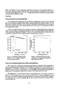
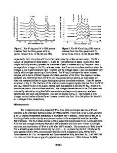
Indium tin oxide films were deposited onto glass substrates at room temperature using reactive dc magnetron sputtering from a 9.8 wt% SnO2 ceramic target. The optimum oxygen content in the sputter gas during processing was established in the usual manner by locating the minimum in the resistivity versus oxygen flow curve. This resistivity minimum is (for this sputter apparatus process) located at 0.1 vol% O2 and represents an optimum in film stoichiometry for the amorphous structure. Sets of samples were produced whose oxygen content lay on either side of this value. These low- and high- oxygen samples were created using, respectively, a 0 and 2 vol % oxygen sputter gas. A sputter target power density of 0.2 W/cm2 at 260 V and a total sputter gas pressure of 10 mTorr were used to deposit 200 nm thick films at a rate of 0.1 nm/s. Film stress was measured during isothermal annealing in air at 250oC using in-situ MOSS measurements. MOSS is a laser-based meth
Data Loading...