Stress Induced During the Solid-Phase Crystallization of Amorphous Silicon Deposited by LPCVD
- PDF / 362,030 Bytes
- 6 Pages / 414.72 x 648 pts Page_size
- 53 Downloads / 324 Views
(SPC) was studied by in-situ monitoring of the film conductance at the annealing temperature. Electrical conductance between 300 and 573K, optical transmission between 0.35 and 2.5 4.tm, X-ray diffraction, ellipsometry in the 1.7 - 5 eV range and Hall effect measurements are performed to characterize the different samples. RESULTS In-situ conductance at annealing temperature The conductance measurements at the crystallization temperature as a function of the annealing time, performed on the amorphous films, show a typical crystallization behavior (Figure 1): at the beginning, a slightly increasing or nearly constant conductance corresponding to the amorphous phase; then a high increase due to the grain growth and a final saturation considered as the end of the crystallization process. A surprising slight decrease of the conductance is however observed after the saturation step. It may be seen in doped or undoped films as well as when a crystallized-deposited film is annealed at the crystallization temperature (Figure 2). Hence, a too long annealing leads to a decrease of the conductance of amorphous or crystallized, doped or undoped deposited layers. 1.0
1.0 doped 00 c
-o" S0.60 w0
0. 0.6-
>o• N
cDo
.N,-
'•E" E 0.2 0 z 0.0
0.4- S0.40.2-
0
z
Undoped 0
200
400
0.0 600
0
800
50
100
150
Annealing time (mn)
Annealing time (mn) Figure 1: Normalized variation of the conductance of amorphous-deposited films measured at 600' C.
Figure 2: Normalized variation of the conductance of a crystallized-deposited film measured at 600' C.
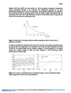
Conductivity-temperature characteristic at different annealing times The conductivity of amorphous-deposited undoped films as a function of the temperature in Arrhenius plots isp resented in Figure 3. The conductivity of unannealed film (0) presents at low temperature a T-l 4 behavior, characteristic of a variable range hopping conduction mechanism in amorphous materials. After an annealing of 3 or 6 hours at 600TC, the conductivity characteristic is linear in the whole temperature range, which indicates a full crystallization of the film. The characteristic is however curved after a long annealing time, for example 24 hours in Figure 3. This curvature may be due to an extra contribution of a hopping conduction or to a fluctuation of the barrier potential at the grain boundary as described in references [6,7]. Whatever the explanation, the curvature indicates that the film is more structurally disordered with a long-time annealing. 514
10-1 6
10-2 E 10-43 0
"0 "7
24
~0 106_ Q
0
7
10
1.5
2.0
2.5
1000 /Temperature
3.0
3.5
(K-1 )
Figure 3: Conductivity of unannealed (0) and 3h (3), 6h (6), 24h (24) annealed at 600' C amorphous-deposited films. Optical transmission The absorption coefficient a of amorphous-deposited undoped films as a function of photon energy at different annealing times is shown in Figure 4. This behavior is typical of amorphouspolycrystalline phase transition [2]. Usually the gap, called Tauc gap, is determined from an (ahv)-1l 2 - hv plot. A
Data Loading...