Stress in Titanium Disilicide Layers, During and After Formation.
- PDF / 355,541 Bytes
- 6 Pages / 420.48 x 639 pts Page_size
- 89 Downloads / 318 Views
Stress in Titanium disilicide layers, during and after formation. J.F. Jongste, F.E. Prins, G.C.A.M. Janssen and S. Radelaar, Centre for Submicron Technology, Delft University of Technology, P.O. Box 5046, 2600 GA Delft, the Netherlands.
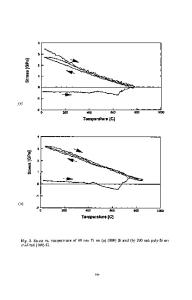
INTRODUCTION During and after formation of a thin layer of titanium disilicide (TiSi2) on a silicon substrate stress is caused in several ways: Intrinsic stresses are due to the deposition process or to phase transformations and grain growth of the deposited material. Extrinsic stresses are caused by thermal effects: the difference in linear thermal expansion coefficients of the layer and the substrate respectively. Problems related to stresses can occur in semiconductor device fabrication. Stresses can deteriorate gate oxides in MOSFETs and can cause cracks in interconnect lines. Also, focusing problems in lithographic steps can occur because of wafer warpage. In this paper some examples of the different types of stress that can occur are shown and discussed. Both multilayer and self aligned Ti-Si samples have been studied: The advantage of the use of Ti-Si multilayers to produce TiSi 2 is that diffusion has to proceed only over a short distance i.e., the multilayer period. So the annealing time can be short. In the self aligned silicidation process, where a layer of a titanium layer on top of a silicon substrate is annealed, the diffusion length is equal to the thickness of the Ti layer. Because longer annealing times are needed, the latter type is used to monitor stress during formation. STRESSES Intrinsic stress may arise from various processes taking place in the deposited layer. Thornton [1] discussed a qualitative structure zone model to describe stress development during sputter deposition. Depending on the deposition conditions (i.e. pressure, substrate temperature, amount of entrapped gas, ion bombardment during sputtering) the stress in the deposited layer can be tensile or compressive. Another mechanism is the change of volume caused by phase transformations of the deposited material. If the layer can not adapt to its new dimensions because of low atomic mobility, stress will result. Extrinsic thermal stress is caused by elastic deformation due to a difference in linear thermal expansion coefficients of the layer and the substrate. The thermal stress in a TiSi 2 layer, formed on a silicon substrate at an elevated temperature, is given by Eq.(l):
0 //= 1 with
El: VI:
al ,a•: AT:
- (a 1-as) AT
(1)
Young's modulus of the layer, Poisson's ratio of the layer, the thermal expansion coefficients of layer and substrate respectively temperature difference between annealing temperature and observation temperature.
Mat.Res. Soc. Symp. Proc. Vol.130. 0199 Malwerals Research Society
322
MEASUREMENT OF STRESS In 1909 Stoney [2] derived an equation (2) describing the stress in thin films, parallel to the substrate:
Es
1(2)
6(1-v,) ti R With
ES: Vs: t 1,t s: R:
Young's modulus of the substrate, Poisson's ratio of the substrate, thickness of layer and substrate the radiu
Data Loading...


