Hybrid Valence Bands in Strained-Layer Heterostructures grown on Relaxed SiGe Virtual Substrates
- PDF / 586,032 Bytes
- 6 Pages / 612 x 792 pts (letter) Page_size
- 87 Downloads / 321 Views
G1.10.1/D4.10.1
Hybrid Valence Bands in Strained-Layer Heterostructures grown on Relaxed SiGe Virtual Substrates
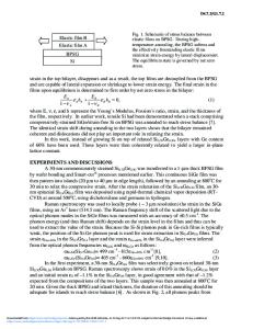
Minjoo L. Lee and Eugene A. Fitzgerald Department of Materials Science and Engineering Massachusetts Institute of Technology Cambridge, MA 02139, USA ABSTRACT The use of alternative channel materials such as germanium [1,2] and strained silicon (ε-Si) [3-5] is increasingly being considered as a method for improving the performance of MOSFETs. While ε-Si grown on relaxed Si1-xGex is drawing closer to widespread commercialization, it is currently believed that almost all of the performance benefit in CMOS implementations will derive from the enhanced mobility of the n-MOSFET [5]. In this paper, we demonstrate that ε-Si p-MOSFETs can be engineered to exhibit mobility enhancements that increase or remain constant as a function of inversion density. We have also designed and fabricated ε-Si / ε-Ge dual-channel p-MOSFETs exhibiting mobility enhancements of 10 times. These p-MOSFETs can be integrated on the same wafers as ε-Si n-MOSFETs, making symmetric-mobility CMOS possible. INTRODUCTION ε-Si p-MOSFETs demonstrate enhanced effective hole mobility (µ eff) compared to bulk Si devices, but the enhancement has widely been observed to degrade under strong inversion conditions (Figure 1) [3-5]. The perpendicular component of the hole wave function, Ψh(z), can propagate over longer distances in ε-Si than in bulk Si due to the strain-induced reduction of the out-of-plane effective mass. By growing thin ε-Si on Ge-rich Si1-xGex, holes sample a hybrid valence band that may improve the mobility characteristics in p-MOSFETs. We have also extensively studied dual-channel heterostructures consisting of strained Ge (ε-Ge) capped with εSi. Very large enhancements are available in p-MOSFETs fabricated from such heterostructures due to the high hole mobility of ε-Ge [6]. Still, we demonstrate that careful engineering of the layer structure is required in order to attain optimum results. EXPERIMENT All heterostructures and Si1-xGex virtual substrates were grown via ultrahigh vacuum chemical vapor deposition (UHVCVD). MOSFETs were fabricated using a short-flow process [4] that utilized a thick, low-temperature SiO2 gate dielectric. A low thermal budget was maintained throughout processing in order to prevent interdiffusion of layers; the maximum time-temperature step was 600°C for 30 minutes to activate the source-drain-gate implant. Ionized-impurity scattering is minimal in all devices since the channels were doped at levels less than 1016/cm3. Mobility characteristics were extracted from the linear-regime transfer characteristics (source current vs gate voltage), and the inversion density, Ninv, was deduced from capacitance-voltage measurements.
Mobility enhancement over bulk Si
G1.10.2/D4.10.2
1.6 1.5 1.4 1.3 ε-Si on Si0.55Ge0.45
1.2
ε-Si on Si0.8Ge0.2
1.1
ε-Si on Si0.7Ge0.3
0.0
12
5.0x10 2 Ninv per cm
13
1.0x10
Figure 1. Hole mobility enhancement versus Ninv of ε-Si p-MOSFETs (Si0.8Ge0.2 and Si0.7Ge0.3 data f
Data Loading...