Structural and Electrical Characterisation of Nickel Silicides Contacts on Silicon Carbide
- PDF / 267,214 Bytes
- 6 Pages / 595 x 842 pts (A4) Page_size
- 7 Downloads / 305 Views
STRUCTURAL AND ELECTRICAL CHARACTERISATION OF NICKEL SILICIDES CONTACTS ON SILICON CARBIDE F. La Via#, F. Roccaforte§, V. Raineri#, P. Musumeci*, and L. Calcagno*.
# CNR-IMETEM, Stradale Primosole 50, 95121, Catania, Italy * INFM and Physics Department, Corso Italia 57, 95129, Catania, Italy. § STMicroelectronics, Stradale Primosole 50, 95121 Catania, Italy
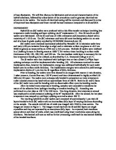
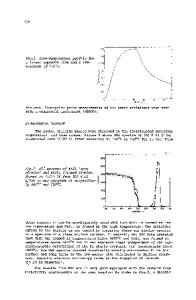
Abstract The interfacial reaction and phase formation as a function of the annealing temperature (600÷1000°C) and times were investigated on nickel thin films evaporated on n type 6H-SiC (0001) substrate. The study was carried out employing a combination of Rutherford Backscattering Spectrometry, X-Ray Diffraction, Transmission Electron Microscopy and sheet resistance measurements. Also several TLM structures and Schottky diodes were fabricated with the same processes and a correlation has been found between the annealing process and the electrical measurements. The only nickel silicide phase that has been observed between 600 and 950 °C was the Ni2Si. The carbon of the consumed silicon carbide layer has been dissolved in the silicide film, during the reaction, forming carbon precipitates. The Ni2Si/SiC Schottky diodes show an almost ideal characteristics (n=1.07) and a barrier height of about 1.3 eV. From the electrical characterisation a non uniform Schottky barrier height seems to be formed.
Introduction Large bandgap semiconductors have been widely investigated and utilised for optoelectronic applications. However, research and commercial interest in large bandgap semiconductor and SiC electrical devices have recently increased due to the availability of high-quality SiC wafers and general advance in material fabrication techniques. SiC is a promising power semiconductor because of its large bandgap (3.0 eV for 6H and 3.2 eV for 4H) and thermal conductivity (4.9 W/cmK for 6H and 4H)1. For power applications, SiC large bandgap translate into a high electrical field and that allows device designs that have lower series resistance and lower power dissipation.2,3 The great potential of SiC as a semiconductor in electronic device applications is challenged by the difficulty of controlling metal contact properties4,5. These properties of the metal/SiC interfaces include uniformity and thickness of the interfacial region, stability at high temperatures, and most importantly the Schottky Barrier Height (SBH). The Schottky barrier height determines the electrical behaviour of an ohmic or Schottky contact. An ohmic contact, important for making outside communication to a device, is defined as having: (a) a linear and symmetric current-voltage relationship for positive and negative voltages; and (b) negligible resistance compared with the bulk of the device. Therefore a low Schottky barrier is necessary to create a good ohmic contact. However, a large SBH is necessary to obtain a good Schottky, or rectifying contact. In both cases, to have good and reproducible metal/silicon carbide contact, a reaction between the metal and the semiconductor is necessary to reduce th
Data Loading...