Structural and Electrical Properties of Heavily-Doped Rapid-thermal-Processed Polysilicon Emitters and Contacts on Silic
- PDF / 852,569 Bytes
- 6 Pages / 420.48 x 639 pts Page_size
- 87 Downloads / 350 Views
STRUCTURAL AND ELECTRICAL PROPERTIES OF HEAVILY-DOPED RAPIDTHERMAL-PROCESSED POLYSILICON EMITTERS AND CONTACTS ON SILICON BRUHA RAICU*, L.A. CHRISTEL**, K.-G. HUANG***, SHIN HASHIMOTO***, W.M. GIBSON***, AND I. WARD**** *Integrated Technologies Associates, 1033 Crestview #307, Mountain View, CA 94040 (now at Monolithic Memories, Inc.) **SERA Solar Corporation, 3151 Jay Street, Santa Clara, CA 95054 ***Physics Department, State University of New York, 1400 Washington Ave., Albany, NY 12222 "****Charles Evans & Associates, 301 Chesapeake Dr., Redwood City, CA 94036
ABSTRACT Supersaturated high-conductivity polycrystalline silicon (polysilicon) formed by rapid thermal processing (RTP) is a promising new material for emitters, contacts and diffusion sources in advanced high-speed bipolar and MOS IC technologies. A matrix of processing conditions was used to evaluate the effect of polysilicon thickness, implant dose, RTP conditions and the nature of the substrate on the dopant diffusion in both the polysilicon and single crystal substrate and also on the interface properties. Results of conductivity measurements, spreading resistance profiling (SRP), secondary ion mass spectroscopy (SIMS), transmission electron microscopy (TEM) and Rutherford backscattering spectroscopy (RBS)/channeling are presented. The results have proved the formation of shallow, defect-free junctions and epitaxial emitters with low series resistance and improved contact properties.
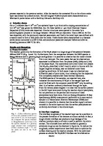
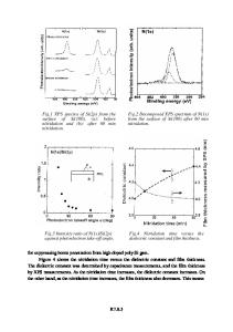
INTRODUCTION In previous work it has been demonstrated that heavy doses of ion implantation followed by RTP can produce very high conductivity polysilicon (p,=4fl/square) [1]. This material has applications for interconnects, low-resistance contacts, high efficiency emitters and diffusion sources for VLSI technology. Difficulties related to the implementation of silicides and polycides in production stimulates a renewed interest in using the new polysilicon process. The first results on the effect of RTP on polysilicon conductivity and structure (secondary grain formation) were published in 1982 [2]. That study showed that phosphorus was more effective than arsenic for high conductivity materials. A detailed study was conducted and a new technology patented [1]. In 1986, based on the above findings, supersaturated polysilicon formed by RTP was used to form low-recombination contacts on n+/p solar cell junctions [3]. A special attention was given to the effect of the process on minority carrier lifetime in silicon with the intent of developing processes with a low thermal budget while maintaining high-quality bulk silicon. Structural and electrical properties at higher phosphorus concentrations and higher annealing temperatures have been also investigated.
Mat. Res. Soc. Symp. Proc. Vol. 106. '1988 Materials Research Society
268
SAMPLE PREPARATION
In [2] it was found that phosphorus-implanted samples had superior conductivity and faster grain growth when compared to arsenic-implanted films under equal processing conditions. As a result we have limited the present s
Data Loading...