Structural and Optical Properties of the Multilayer Structures Formed by Ge Sub-Critical Insertions in a Si Matrix
- PDF / 215,574 Bytes
- 6 Pages / 612 x 792 pts (letter) Page_size
- 4 Downloads / 323 Views
Structural and optical properties of the multilayer structures formed by Ge sub-critical insertions in a Si matrix George E. Cirlin 1,3 , Nikolai D. Zakharov 1, Peter Werner 1, Alexander G. Makarov 2, Andrei F. Tsatsul’nikov 2, Victor M. Ustinov 2, and Nikolai N. Ledentsov 2 , Vyatcheslav A. Egorov 3, and Ulrich Gösele 1 1 Max-Planck-Institute for Microstructure Physics, Halle D-06120, Germany 2 A.F.Ioffe Phisico-Technical Institute RAS, 194021 St.Petersburg, Russia 3 Institute for Analytical Instrumentation RAS, 194021 St.Petersburg, Russia
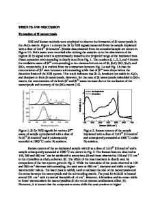
ABSTRACT Si/Ge multilayer structures formed by the deposition of relatively small amounts of Ge layers (less then the critical thickness for 3D islands formation) are obtained by molecular beam epitaxy. Their structural and optical properties are investigated in detail. Appropriate growth parameter of the stacked island structures lead to significant increasing of the luminescence efficiency even at room temperature. INTRODUCTION The strained SiGe/Si system is expected to play an important role in monolithic integration of Si-based opto-and microelectronic devices. It is well known that Ge/Si system is a prominent example of Stranski-Krastanow growth mode, where three-dimensional (3D) islands appear at the surface after exceeding of a certain critical thickness. There are a lot are a lot of investigations in numerous groups (see, e.g., [1,2]. However, already small amounts of deposited Ge (smaller than one monolayer) can form island-like structures. In the present work, we report on the observation of a new kind of nanostructures formed by sub-critical Ge insertions in a Si matrix and their structural and optical properties. Our approach is based on the following assumption: insertion of Ge submonalyers (SML) into Si may lead to the formation of the ensemble of relatively small islands (with lateral sizes less than the hole Bohr radii). This can result in a partial lifting of the selection rule for radiative recombination and exciton formation (which may be stable up to room temperature) via electron and localizedhole interaction. This situation is possible if the Coulomb attraction energy is high enough to localize electrons near the potential barrier which is produced by Ge SML inclusions in the conduction band. In the case of relatively large sizes of QDs or large widths of quantum wells, this barrier may also lead to spatial separation of the electrons and holes [3]. Furthermore, for the SML in other heteroepitaxial systems [4, 5] the narrow photoluminescence (PL) line leads to the increase of the absorption (gain). The PL intensity will also increase if multiple layers are used with Ge SML separated by Si spacers. Due to relatively small strain accumulation in such a system, it is expected that there will be a low probability of dislocations and formation of structural defects. In fact, despite of the total amount of the Ge (sub)monolayers deposited is lower then the critical thickness we show that they exhibit (quasi) 3D properties when capped with a host (Si) material un
Data Loading...