Structural and Spectroscopic Study of Manganese Silicide Islands on Silicon
- PDF / 3,047,847 Bytes
- 6 Pages / 612 x 792 pts (letter) Page_size
- 108 Downloads / 317 Views
STRUCTURAL AND SPECTROSCOPIC STUDY OF MANGANESE SILICIDE ISLANDS ON SILICON Miyoko TANAKA, Qi Zhang, Masaki Takeguchi and Kazuo Furuya National Institute for Materials Science, Sakura, Tsukuba 305-0003, JAPAN
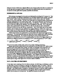
ABSTRACT The Mn deposited clean Si (111) substrates were examined with UHV-TEM and STM that are part of an UHV-TEM/STM integrated characterization system. The Mn deposition with coverages of 5-20 ML followed by annealing at 673 K formed MnSi islands with Moire fringes. They showed metallic character. Subsequent annealing at 873 K dissipated the islands instead of transforming them into MnSi1.7. The re-deposition of Mn and re-annealing at 473 K succeeded to transform MnSi islands into MnSi1.7. The islands had several orientation relationships with substrate Si, and were semiconducting. The growth mechanism of MnSi1.7 is inferred. INTRODUCTION Transition metal silicide-silicon systems have been investigated extensively for both technological and scientific use. Most silicides are metallic and thus are used for contacts, gates, etc [1,2], but some silicides are semiconducting and are potential candidates for silicon-based optoelectronic devices or thermoelectric materials [3]. β-FeSi2 is the most promising material with its light emitting character [4]. A number of studies have been made to investigate its growth mechanism, optical property, structure, and so on [5,6]. On the other hand, MnSi1.7 is another candidate with its direct band gap around 0.7eV and the possibility of epitaxial growth [7]. However, not a lot of studies have been performed to make its structure, growth process, electronic and optical properties clear [8,9]. Only a few papers reported that the formation of MnSi1.7 began at temperatures higher than 773 K, forming through an island growth process [10,11]. In the present work, we report the growth of the Mn silicide islands formed epitaxially on Si (111) by transmission electron microscopy (TEM) and scanning tunneling microscopy (STM) with UHV - TEM/STM combined system. Structure of the Mn silicide islands was investigated depending on the Mn coverage and annealing temperature after the deposition. It was found that MnSi1.7 grew with the re-deposition to MnSi islands and re-annealing at relatively low temperature [12]. Structure of the Mn silicides islands and their properties will be discussed. EXPERIMENT All experiments were done in an UHV-TEM/STM integrated characterization system (UTSICS). UTSICS is a multi-chamber, UHV surface characterization and preparation system that is attached to an UHV-FE-TEM and an UHV-STM. The detail of this system has been described elsewhere [13]. Samples were Si (111) prepared for TEM specimens by mechanical thinning followed by chemical etching, with an etchant HNO3: HF = 9:1, and bulk Si (111) for STM specimens. After being loaded into the UTSICS, samples were prepared in-situ through 2kV Ar ion milling and W9.8.1
resistive heating at 1273 K. Subsequent XPS measurement suggested neither C nor O related peaks. This procedure produces surface area displaying
Data Loading...