Structural Defect-Related Photoluminescence in GaN
- PDF / 259,050 Bytes
- 6 Pages / 612 x 792 pts (letter) Page_size
- 78 Downloads / 387 Views
Y5.55.1
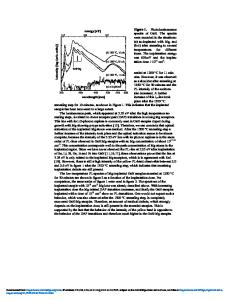
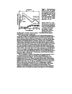
Structural Defect-Related Photoluminescence in GaN L. Chen, B.J. Skromme, M.K. Mikhov, H. Yamane1, M. Aoki1, F.J. DiSalvo2, B. Wagner3, R.F. Davis3, P.A. Grudowski4 and R.D. Dupuis4 Department of Electrical Engineering and Center for Solid State Electronics Research, Arizona State University, Tempe, AZ, 85287-5706, U.S.A. 1 Tohoku University, Sendai 980-8577, Japan 2 Department of Chemistry and Chemical Biology, Cornell University, Ithaca, NY 14853, U.S.A. 3 Department of Materials Science and Engineering, North Carolina State University, Raleigh, NC 27695-7907, U.S.A. 4 Microelectronics Research Center, University of Texas, Austin, TX 78712-1100, U.S.A. ABSTRACT Broad, low temperature photoluminescence (PL) peaks near 3.4-3.42 eV in GaN have previously been associated with basal-plane stacking faults. Recently, we observed unusually sharp and highly structured PL peaks in this region in high quality bulk GaN grown from a Na/Ga flux, some of which display characteristic shifts and narrowing as a function of excitation power. Here, we study these peaks as a function of excitation intensity and crystal polarity, and compare them to those observed in GaN grown on off-axis SiC or sapphire (0001) substrates by metalorganic chemical vapor deposition (MOCVD). In the off-axis material on either substrate, similar peaks are observed to those in the bulk samples. In addition, a low energy peak near 3.21 eV is observed, which does not occur in the bulk material. INTRODUCTION As a developing wide gap semiconductor material, GaN has important applications to both optical and electronic devices. To improve the growth of both heteroepitaxial and bulk material, various studies of structural defects have been performed. In particular, a generally broad low temperature luminescence band near 3.4 eV has frequently been attributed to such defects [1-4]. (This band should be carefully distinguished from sharper peaks at 3.365 and 3.31 eV, which are commonly observed artifacts related to cryostat windows and not to GaN.) A comparison of transmission electron microscopy (TEM) observations and cathodoluminescence spectra of heteroepitaxial GaN samples suggested that the 3.4 eV band is related to basal plane stacking faults [1]. A recent study of ammonothermally grown bulk material using TEM and low temperature photoluminescence (PL) also supports this attribution [5]. The identification of this band has been controversial, however, with other groups assigning it at various times to O impurities [6], dislocations [2], or stacking mismatch boundaries (i.e., non basal plane stacking faults) [4]. The early attribution to O has been strongly questioned [7]. It has been most commonly and consistently observed in samples grown on vicinal SiC or sapphire (0001) substrates [1, 8]. Here, we study this feature in bulk GaN crystals grown by the Na/Ga flux method, where it exhibits a complex and highly variable fine structure. We also study similar features in heteroepitaxial GaN layers grown on off-axis SiC or sapphire substrates by MOCVD. A
Data Loading...