Structure of The Annealed Au-Si(100) System: A Uhv-Hrem Study
- PDF / 2,801,012 Bytes
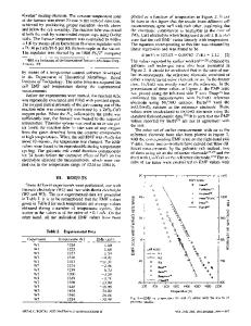
- 5 Pages / 414.72 x 648 pts Page_size
- 77 Downloads / 251 Views
G. JAYARAM AND L. D. MARKS Department of Materials Science and Engineering, Northwestern University Evanston, I1L 60208
ABSTRACT The structure -obtained on annealing sub-monolayer of Au deposited on clean Si(100) surfaces at room temperature was studied using mainly ultrahigh vacuum transmission electron imaging (UHV-HREM). Spots suggesting a 5x1I type reconstruction and faint 1/2 order streaks were seen in the diffraction patterns. The reconstructed wave shows pairs of Au-rows which correspond to the"tecs"reported in an earlier STM study. Lateral disorder across the rows was seen to be responsible for the streaks in the patterns. INTRODUCTION Interfaces in metal - semiconductor systems play a critical role in determining the electronic properties of the device. In this regard, characterization of the interfacial microstructure and chemistry in these systems are extremely crucial. AuISi(100) interface has been a model system for study of Schottky barrier formation; spectroscopy studies have shown that when Au above a certain critical thickness value (the value is a subject of dispute) is deposited on clean Si(100) surfaces, reaction commences at room temperature itself resulting in a mixed interface [1-3]. Structural information has been obtained mainly from LEED [3-6] investigations; these report that LEED patterns show a decrease in the intensity of Si(100) reconstruction spots on Au deposition at room temperature followed by the appearance of a Au-silicide ring at higher coverages. Superstructure spots corresponding to different Auinduced Si surface reconstructions are seen on annealing such a system e.g. a c(8x2) type pattern which transforms to a N'26x1I and Ný26x3 pattern (and 1/3 or 1/2 order streaks) at higher temperatures [4-5] and a 5x1 type pattern [6] have all been reported. However, despite reports of these reconstructions, a detailed atomic picture is still lacking: there is only one STM study [7] that has attempted to resolve the details of the 5x3 and ql26x3 phases. The study reports the presence of "stripes"separated by "trenches". Atomic scale features are reported to exist both on the stripes and in the trenches, the arrangement of those on the stripes was responsible for the inter-stripe periodicity corresponding to either the "15"t or "4126" type. While the study did provide a real space picture of the reconstruction, it suffered from the drawback that it could not identify the features i.e. Au or Si. The current study attempts to understand the nature of these features in the annealed Au-Si(100) system usIing mainly high resolution transmission electron microscope imaging and diffraction. EXPERIMENTAL PROCEDURE Thin samples of p-type Si(100) (B3doped at 1 ohm-cm) were mechanically polished, 275 Mat. Res. Soc. Symp. Proc. Vol. 355 01995 Materials Research Society
slightly dimpled and chemically thinned in a 10% HF + 90% HN0 3 solution before being transferred -into a UHV - surface science chamber atta~ched to a Hitachi UHV-H9000 electron microscope [8] (which was operated at 300 kV and 250 k
Data Loading...