A Study of the Deactivation of High Concentration, Laser Annealed Dopant Profiles in Silicon
- PDF / 59,327 Bytes
- 6 Pages / 612 x 792 pts (letter) Page_size
- 115 Downloads / 298 Views
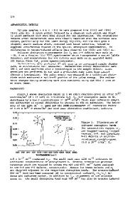
A Study of the Deactivation of High Concentration, Laser Annealed Dopant Profiles in Silicon Yayoi Takamura, Sameer Jain, Peter B. Griffin, James D. Plummer Center for Integrated Systems, Stanford University, Stanford, CA, 94305 ABSTRACT As semiconductor device dimensions continue to decrease, the main challenge in the area of junction formation involves decreasing the junction depth while simultaneously increasing the active dopant concentration. Laser annealing is being investigated as an alternative to rapid thermal annealing (RTA) to repair the damage from ion implantation and to activate the dopants. With this technique, uniform, box-shaped profiles are obtained, with dopant concentrations that can exceed equilibrium solubility limits. Unfortunately, these super-saturated dopant concentrations exist in a metastable state and deactivate upon further thermal processing. In this work, a comprehensive study of the deactivation kinetics of common dopants (P, B, and Sb) was performed across a range of annealing conditions. For comparison, As deactivation data from the work of Rousseau et al.1 is also presented. Each dopant exhibits different deactivation behavior, however, As and P can be classified as unstable species while B and Sb are stable against deactivation until higher temperatures of 700-800ºC. In addition, a means of maintaining these metastably doped layers is being investigated with the goal of meeting the International Technology Roadmap for Semiconductors (ITRS) requirements for ultrashallow junctions. INTRODUCTION The size of the Metal – Oxide – Semiconductor (MOS) transistor has been scaled aggressively as semiconductor manufacturers strive to create faster microprocessors with more functionality. In the area of front-end technology, this rapid scaling translates to major obstacles with the thin gate oxides and the formation of the highly doped junctions at the source and drain. In the latter category, the lateral abruptness of the dopant profiles needs to be increased with a simultaneous decrease in the junction depth and the sheet resistance of these doped regions. Current technology uses a two-step process of ion implantation followed by rapid thermal annealing (RTA) to introduce and electrically activate dopants. Electrical solubility of the dopants, which is on the order of 2-3x1020 cm-3, limits the active dopant concentrations. Once this limit is reached, a fundamental tradeoff exists between decreasing junction depth and increasing sheet resistance. Laser annealing is being studied as a possible alternative to RTA. With laser annealing, a pulsed laser melts the near surface region of the silicon crystal for durations of about 70ns. The non-equilibrium nature of the liquid phase epitaxy provides for several advantages over conventional techniques. First, the dopant diffusivities in the liquid silicon are 108 times greater than that in solid silicon, allowing the dopants to diffuse throughout the molten region. Second, the liquid-to-solid regrowth front travels so fast that the dopant atoms are
Data Loading...