Study of Microstructure and Gas Sensing Properties of Tin Oxide Thin Films Prepared by Metal Organic Chemical Vapor Depo
- PDF / 344,019 Bytes
- 6 Pages / 414.72 x 648 pts Page_size
- 79 Downloads / 372 Views
Mat. Res. Soc. Symp. Proc. Vol. 415 ©1996 Materials Research Society
temperature, etc. In case of our study, MOCVD technique has been applied for the production of undoped SnO2 thin films to study their behavior in both air and reducing gas atmosphere in relation with the microstructure. The advantage of the MOCVD technique are easy control of exclusion and/or inclusion of foreign species and large throughput up to commercial quantity. EXPERIMENTAL Polycrystalline SnO2 thin films were prepared on alum in a po lycry stallin e The films were substrates. grown in a cold-wall, horizontal, low-pressure MOCVD system equipped with a pyrolytic in a graphite resistor encased pyrolytic boron nitride heater. available Commercially tetraethyltin, Sn(C2H 5 )4, was
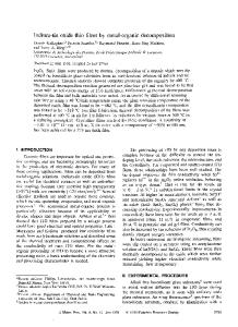
•,WoF 'l.m ..
V7 e_
-
W-
H
M.C
M
C
used as the organometallic (OM)
source.
The
OM
precursor was maintained at 19 'C by circulating running water
... So-I
around a precursor evaporator and its vapor was transported into a reactor by ultra high purity N 2 as the carrier gas. Ultra high purity 02 was injected using a separate delivery line into the reactor as the oxidant. The OM precursor delivery line and the inlet flange were heated and maintained at 130 'C to prevent condensation of the OM precursor vapor phase. A schematic diagram of the MOCVD apparatus used in this experiment is shown in Detailed growth Figure 1. parameters are summarized in table 1.
|
troler
Figure 1. Schematic diagram of MOCVD apparatus
Table 1. Summary of deposition parameters. Substrate material: Reactor pressure: OM source temperature:
alumina 40 Torr 19 °C
Growth temperature: Oxygen flow rate: OM source flow rate:
238
600 0C 200 sccm 6-30 sccm
The film structure and crystallinity were determined by x-ray diffraction (XRD). The surface microstructure was examined by scanning electron microscopy (SEM). Auger electron spectroscopy (AES) was also performed to obtain chemical information of the films. After deposition process, the samples were placed in a box furnace operated at 550 'C in air for 7 hours. This subsequent annealing was to promote removal of surface contamination and achieve a controlled concentration of oxygen vacancy defects.[2] For sensing test purpose, four platinum electrodes, two outer ones for the current supply and two inner ones for measurement of the voltage drop across them, were attached to the film surface. The distance between the inner electrodes is approximately 3 mm. Then the films were introduced into an alumina tube placed onto a horizontal furnace to measure the electrical resistance as a function of temperature. The measurement was carried outf under both dry air and 1% H2 environmental condition with a fixed amount of flow rate, 10 sccm, from 500 'C to 100 'C on cooling. RESULTS AND DISCUSSION 2500
X-ray 0-20 scan of these samples shown in Figure 2 revealed that all films were composed of tetragonal rutile structure SnO2 phase. These films exhibited no particular preferred crystallographic growing directions. The XRD intensity profile
Data Loading...