Study of the Influence of Structural Properties on Si and Be Doping of Heteroepitaxial InAsSb on GaAs-Coated Si Substrat
- PDF / 2,197,077 Bytes
- 6 Pages / 420.48 x 639 pts Page_size
- 81 Downloads / 289 Views
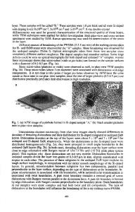
STUDY OF THE TNFLUENCE OF STRUCTURAL PROPERTIES ON Si AND Be DOPING OF HETEROEPITAXIAL InAsSb ON GaAs-COATED Si SUBSTRATES FOR INFRARED PHOTODIODES J. DE BOECK, W. DOBBELAERE, M. VAN HOVE, J. VANHELLEMONT, W. DE RAEDT, W. VANDERVORST, R. MERTENS and G. BORGHS Interuniversity Micro Electronics Center (IMEC vzw.), 75 Kapeldreef, B-3030 Leuven; Belgium ABSTRACT The behavior of Si and Be impurities in InAs Sb, (0.051.5ixm) and optimised GaAs buffer, using SLS's and annealing sequences, is necessary when device isolation is required. Another effect inherent to heteroepitaxy is the degradation of transport properties of the epilayer. Different studies" on InAs heteroepitaxy argue for the presence of an n-type accumulation layer at the interface and/or mobility decrease towards the interface. We investigated the situation in our samples by stripping Hall measurements. We simulated the expected sheet Hall coefficient RHs and sheet resistivity Rs depth profile for different g.t-n profiles of the epilayer, using an analytical model" for multilayer structures. The results of these simulations are compared with the measured values to estimate the real ji-n profile. Figure 4 compares the results of this procedure for a thick undoped InAsSb layer (#S 1) grown on a thin GaAs buffer on Si. The measured values are represented by the markers, for covenience ( -RHs) is plotted. The lines marked 'u' in the figure represent the simulation of a uniform Ix-n profile using the values of the differential gIand n obtained from stripping Hall measurements. The initial value of RHs and Rs are reasonably well fitted using this model but the shape of the simulated depth profile disagrees with the measurement. To obtain a good fit to the RHs-Rs depth profiles (solid line through the markers), we model the carrier density profile by an exponential increase and the mobility by a linear decrease toward the interface. We note that these ungated Hall measurements are unable to decide between the effect of the interface and the surface layer. But taking into account the low values reported for n-type surface accumulation (5x1012 cm"2 ) in MBE InAs on GaAs (ref 11) , we assume that the interface region represents a dominant influence on the electrical properties. The interface carrier density and its decay is related to impurity diffusion from the substrate and the presence of electrically active defects in the interface region. Simulations of layers on GaAs substrates revealed a lower carrier density. The dislocation structure is responsible for the mobility decrease, evident below 2 to 3 gxfrom the interface. Structural properties and diode performance We already demonstrated the possibility to fabricate metallurgical p-n junctions in the heteroepitaxial InAsSb using Be and Si. Using this knowledge, we grew several diode
151
structures in InAs and InAsSb to investigate the electrical performance of the junctions. Figure 5 gives I-V curves for two different diodes. Curve a) is the characteristic of an InAs p-'i'-n diode, curve b) represents a p-'i'
Data Loading...