Submicrometer Technique Etches Curvilinear Silicon and Glass Patterns with HF-Saturated Hydrogel Stamps
- PDF / 126,731 Bytes
- 1 Pages / 589.616 x 784.16 pts Page_size
- 111 Downloads / 217 Views
10/31/2006
12:52 PM
Page 856
RESEARCH/RESEARCHERS
properties of the 2D structures by measuring the specular reflection of light as a function of the wavelength of the incident field, observing a dip at 1100 nm, corresponding to the third-order Bragg reflection band. The researchers also demonstrated the potential of the 2D array of KTiOPO4 rods to host an efficient nonlinear interaction by measurements of the diffracted light at the second-harmonic frequency of the incident wave. This procedure enables control over the direction of growth relative to the orientation of the 2D structure. For any given application, it will then be possible to use the most appropriate combination of nonlinear or electro-optic coefficients of the material, something which is not always possible in bulk KTiOPO4, given the limited material birefringence. Such newly developed photonic crystals, which should be easily integrated in siliconbased devices, may find applications in generating light more efficiently at higher frequencies, in the electro-optic modulation of light, and in obtaining backward parametric amplification and oscillation.
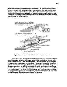
Submicrometer Technique Etches Curvilinear Silicon and Glass Patterns with HF-Saturated Hydrogel Stamps Applications in micro-optics, microfluidics, and microelectronics call for micrometer-sized devices with curvilinear or multilevel surface topographies. Casting elastomers against rigid masters is a parallel process that can rapidly create such architectures, but the resulting polymeric devices possess low resistance to mechanical wear, are permeable to gases, and often swell when exposed to organic solvents. Durable inorganic substrates, with better mechanical and chemical properties, may be patterned by expensive techniques such as reactive ion etching, laser ablation, or micromachining, but the throughput rate of these serial processes is low. In the July 16 issue of Advanced Materials (p. 2004; DOI: 10.1002/adma.200600716), followed by a recent publication in Chemistry of Materials (p. 4722; DOI: 10.1021/ cm061468p), researchers at Northwestern University, led by B.A. Grzybowski, have presented a novel, inexpensive, directprinting technique that is suitable for rapid prototyping of multilevel reliefs in a variety of rigid substrates. The technique boasts a lateral resolution (in silicon) of several hundred nanometers, and it can pattern several square centimeters at a time. Using soft lithographic techniques, Grzybowski and co-workers created a flexible hydrogel stamp by first patterning a reusable micropatterned master 856
Figure 1. Schematic illustration of the experimental procedure for reactiondiffusion microetching.
a
b
c
with the desired topography, then casting high-gel-strength agarose against it. They “inked” the agarose stamp by soaking it for 4 h in a 0.6 M aqueous solution of hydrofluoric acid, with 0.1 vol% Triton X-100 surfactant. The researchers laid the saturated stamp, feature side up, in light mineral oil, which confined the etchant to the raised features and reduced e
Data Loading...