Effects of Substrate Parameters on Amorphous-Crystalline Silicon Interface
- PDF / 281,835 Bytes
- 6 Pages / 420.48 x 639 pts Page_size
- 12 Downloads / 359 Views
EFFECTS OF SUBSTRATE PARAMETERS ON AMORPHOUS-CRYSTALLINE SILICON INTERFACE
U. BESI VETRELLA* AND J. D. COHEN** *ENEA-CRIF, 80055 Portici (NA), ITALY "**University of Oregon, Department of Physics, Eugene,, OR 97403, USA
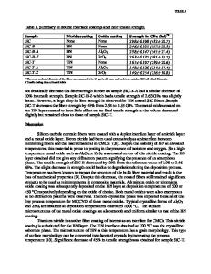
ABSTRACT Capacitance vs. temperature, deep-level transient spectroscopy (DLTS), and transient photocapacitance spectroscopy have been used to investigate the amorphous-crystalline silicon interface region of a device made of hydrogenated amorphous silicon deposited on a lightly doped n-type crystalline silicon. By comparing our results between substrates with and without oxide contamination with those in a earlier study, we have been able to correlate the effects of substrate preparation on the density of interface states. INTRODUCTION Junction capacitance measurements have been successfully used on hydrogenated amorphous silicon to provide a clear picture of the bulk density of states (1), and to gain new insight about such effects, as the study of light-induced metastable defects (2) or the effect of incorporation of impurities (3). More recently such techniques were applied to a device consisting of a palladium Schottky barrier deposited on a sub-micron thick amorphous silicon layer grown on a lightly doped n-type crystalline silicon substrate. This simple device structure has provided a powerful tool for the study of the electronic states at the interface between amorphous and crystalline silicon. Results from these studies previously published (4,5) indicate that: - There is an interface region that extends for about 350 Angstrom from the crystalline substrate with a high defect density (about 1018 cm- 3 ) and a shallow Fermi level. - The density of states of this region is Gaussian shaped and is centered 0.88 eV below the conduction band. - A very small offset (AE < 50 meV) is exhibited for conduction bands, while an offset of 0.58 eV exists at valence bands. Although the picture described above appears reasonably complete, many questions have been left unanswered such as the effect of substrate cleaning or surface orientation on the interface states. This research area would appear to be very important due to the growing interest in the applications of amorphous silicon in microelectronics. In this paper, we will present data that begins to address one of these issues: the effect of cleaning procedures (i.e. presence or absence of an oxide layer) on the density of states at the interface. SAMPLE PREPARATION Samples were deposited in a capacitively coupled glow discharge system using a 50% silane/50% argon gas mixture; substrate temperature was 250 °C and an rf power 3 Watt. Prior to deposition, n-type crystalline silicon substrates were chemically cleaned and a controlled amount of oxide, about 10 Angstrom thick, was grown on them. To remove the oxide layer, some substrates were etched in HF for about 2 minutes immediately before growth; hydrogen and/or fluorine atoms remain
Mat. Res. Soc. Symp. Proc. Vol. 219. ©1991 Materials Research Society
820
bound to the surface instead of oxigen,
Data Loading...