Surfactants in Controlling Removal Rates and Selectivity in Barrier Slurry for Cu CMP
- PDF / 117,800 Bytes
- 6 Pages / 612 x 792 pts (letter) Page_size
- 4 Downloads / 298 Views
0991-C09-03
Surfactants in Controlling Removal Rates and Selectivity in Barrier Slurry for Cu CMP Jinru Bian CMP Technologies, Rohm and Haas Electronic Materials, 451 Bellevue Road, Newark, DE, 19713
ABSTRACT Leading edge integrated circuits (ICs) are complicated structures designed to have up to 3 capping layers above a low k dielectric material. The upper capping layer may use TEOS and/or silicon nitride (SiN), while the lower one may use silicon carbon nitride (SiCN), silicon carbide (SiC), or carbon doped oxide (CDO) immediately above the low k dielectric. Therefore, a barrier slurry for copper CMP, in addition to exhibiting a high removal rate of the barrier, must be able to remove the upper capping layer and stop at the underlying dielectric surface. We have developed a slurry family that can effectively remove TaN, TEOS, SiN, CDO, and/or SiCN, or any combination of these films, or can stop at any one or two film surfaces of TEOS, SiN, CDO, SiCN, and SiC, depending on the specific slurry design. Removal rate control is achieved by one or two additives. One of the additives is an anionic surfactant. When selecting a surfactant, the surfactant hydrophobicity and charge interaction between the surfactant and the wafer surface are two important factors to be considered. This report discusses these two factors in selecting a proper surfactant for a specific slurry application. INTRODUCTION One of the critical requirements in the production of increasingly complex and dense semiconductor structures is the ability to retain planarity. Without the ability to planarize, the complexity and density of the structures constructed on a semiconductor wafer are greatly limited. Chemical Mechanical Planarization (CMP) is an enabling technology in this area and has proven to be the most effective method to planarize surface films on semiconductor substrates. Copper CMP generally employs a two-step polishing process. In the first step, Cu slurry is used to remove the bulk copper film layer and any remaining Cu residue, while maintaining good planarization across the wafer. The second step is used for removal of a barrier film such as tantalum (Ta) or tantalum nitride (TaN) while maintaining and preferably improving topography There may be one, two or three capping layers between the barrier layer and the low-k dielectric. The top capping layers may be used for the purpose of topography correction and a lower capping layer can be used as a polishing stop layer to protect the underlying dielectric from chemical and mechanical damage. An additional layer may be designed for specific integration purposes. The top layer immediately below the barrier film may be silicon nitride (SiN) or TEOS SiO2 (TEOS), whereas the lower layer immediately above the dielectric may be TEOS, silicon carbide (SiC), silicon carbide nitride (SiCN) or SiN. The low k dielectric itself, usually carbon doped oxide (CDO), can also be used as a stopping layer. Therefore, in addition to removing the barrier film, a barrier slurry may be required to remove the t
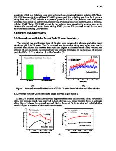
Data Loading...