Synthesis of Crystalline Silicon Nanoparticles in Low-Pressure Inductive Plasmas
- PDF / 951,757 Bytes
- 6 Pages / 612 x 792 pts (letter) Page_size
- 9 Downloads / 282 Views
F1.10.1
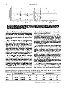
Synthesis of Crystalline Silicon Nanoparticles in Low-Pressure Inductive Plasmas Ameya Bapat1, Uwe Kortshagen1, Stephen A. Campbell2, Christopher R. Perrey3, C. Barry Carter3 1 Department of Mechanical Engineering 2 Department of Electrical and Computer Engineering 3 Department of Chemical Engineering and Materials Science University of Minnesota, Minneapolis, MN 55455 ABSTRACT Amorphous silicon has been used for a wide variety of electronic applications including thin film transistors and energy conversion devices. However, these devices suffer greatly from defect scattering and recombination. A method for depositing crystalline silicon would be highly desirable, especially if it can be remotely created and deposited on any kind of substrate. Our work aims at synthesis and deposition of mono-disperse, single crystal silicon nanoparticles, several tens of nm in diameter on varied substrates. Synthesis of nanocrystals of 2-10 nm diameter has been previously reported but larger particles were amorphous or polycrystalline. This work reports the use of an inductively coupled low-pressure plasma to produce nanocrystals with diameters between 20-80 nm. Electron microscopy studies confirm that the nanocrystals are highly oriented diamond-cubic silicon. INTRODUCTION Recently, experimental studies on nanoparticle formation have attracted significant interest. Potential applications of crystalline nanoparticles for optical and quantum effect devices have led to intense research efforts in that direction (see ref. (1) and references therein). These efforts have mainly focused on particles in the 2-10 nm range for their unique confinement effects and ease of production. As a prominent example, microelectronic memory devices have already been built using silicon nanocrystals in this size range (2). Single-crystal semiconductor nanoparticles with high carrier velocities and longer recombinative lifetimes are very well suited for device fabrication and are of particular interest. Out of a variety of synthesis methods, gas-phase synthesis of nanoparticles has been widely used for electronic applications due to the high degree of purity that can be achieved. A variety of gasphase processes such as inert gas condensation (3), flame synthesis (4), furnace flow reactors (5) and thermal plasma particle synthesis (6) have been proposed for nanoparticle synthesis. These processes are relatively efficient in the synthesis of particles, however, they often produce either agglomerates or nanoparticles with broad size distributions that require post-synthesis size selection (2, 7). Nanocrystals with size of the order of a few tens of nanometers having a monodisperse size distribution would be best suited for use with present day commercial lithography tools. Recently several groups studying the formation of silicon particles in silane plasmas have reported generation of monodisperse, non-agglomerated distributions of particles (8-11). However, particles observed in these studies were amorphous. The monodispersity of the particle form
Data Loading...