Synthesizing Nanocrystalline Carbon Thin Films by Hot Filament Chemical Vapor Deposition and Controlling Their Microstru
- PDF / 525,117 Bytes
- 14 Pages / 612 x 792 pts (letter) Page_size
- 9 Downloads / 352 Views
B.R. Weiner Department of Chemistry, University of Puerto Rico, San Juan, PO Box 23346, PR00931, U.S.A.
G. Morell Department of Physical Sciences, University of Puerto Rico, San Juan, PO Box 23323, PR00931, U.S.A. (Received 21 December 2001; accepted 29 April 2002)
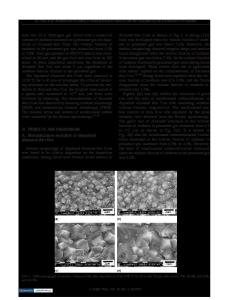
Nanocrystalline carbon (n-C) thin films were deposited on Mo substrates using methane (CH4) and hydrogen (H2) by the hot-filament chemical vapor deposition (HFCVD) technique. Process parameters relevant to the secondary nucleation rate were systematically varied (0.3–2.0% methane concentrations, 700–900 °C deposition temperatures, and continuous forward and reverse bias during growth) to study the corresponding variations in film microstructure. Standard nondestructive complementary characterization tools such as scanning electron microscopy, x-ray diffraction, atomic force microscopy, Raman spectroscopy, and x-ray photoelectron spectroscopy were utilized to obtain a coherent and comprehensive picture of the microstructure of these films. Through these studies we obtained an integral picture of the material grown and learned how to control key material properties such as surface morphology (faceted versus evenly smooth), grain size (microcrystalline versus nanocrystalline), surface roughness (from rough 150 rms to smooth 70 rms), and bonding configuration (sp3 C versus sp2 C), which result in physical properties relevant for several technological applications. These findings also indicate that there exist fundamental differences between HFCVD and microwave CVD (MWCVD) for methane concentrations above 1%, whereas some similarities are drawn among films grown by ion-beam assisted deposition, HFCVD assisted by low-energy particle bombardment, and MWCVD using noble gas in replacement of traditionally used hydrogen.
I. INTRODUCTION
The metastable allotrope of carbon known as diamond is a unique and promising material, which engenders excitement and interest. Diamond thin films are attractive for several mechanical, optical, and electronic applications such as in tribological coatings and cutting tools, heat sinks,1 optical windows (wide band gap, 5.45 eV),2 high-temperature and high-power electronics (breakdown voltage of 107 V/cm), microsensors, biosensors,3,4 vacuum microelectronics in general, and field emission arrays in particular,5 and therefore, diamond is considered as an engineering material. The promise of diamond a)
Address all correspondence to this author. [email protected] b) National Science Foundation Graduate Fellow. 1820
http://journals.cambridge.org
J. Mater. Res., Vol. 17, No. 7, Jul 2002 Downloaded: 25 Mar 2015
stems from the coexistence of several superlative properties such as extreme hardness, chemical inertness, high thermal conductivity, and wide spectral transparency, to name a few.6–8 Intense research efforts over the past two decades have yielded the technology to grow high-quality diamond thin films on nondiamond substrates,9 thus enabling some of these applications above mentioned. A variety of diamond chemical
Data Loading...