The Characterisation of The Compositional and Electronic Profiles of Delta-Doped Layers Using Transmission Electron Micr
- PDF / 1,585,393 Bytes
- 6 Pages / 414.72 x 648 pts Page_size
- 81 Downloads / 282 Views
Mat. Res. Soc. Symp. Proc. Vol. 354 0 1995 Materials Research Society
720E
360HW
m0IF5
GaAs - Si bilayer
GaAs - Si monolayer
I~
-360 ~ -72-0
124nm
GaAs a)
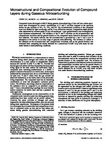
Fig.2. Line profiles from five images in the through-focal series of a) a Si monolayer and b) a Si bilayer in GaAs, with the intensity projected parallel to the layers at the defoci (nm) indicated and at a crystal thickness of 15Onm.
Fig. I. One image from a through-focal series of a Si monolayer and bilayer in GaAs, taken at 200kV 3.9"
from [1101 (with the layers vertical), at 1500nm underfocus.
al
b)
First fringe spacing d (nm)
3.0-
-. ,.
""Simulation: - - 2 unit cells of Si unit cells of.3Si -.*-Expt. (bilayer
1.01
Wzad monolayer)
.
'-s60
'-4&
'
0
410 ' 800
400 800 Defocus (nm)
Defocus (nm)
Fig.3. a) Graphs of first fringe spacing, showing that both the monolayer and bilayer have mean
compositional widths of 2.5 unit cells; b) Graphs of first fringe contrast showing that the bilayer has approximately twice the contrast of the monolayer. The form of the graphs (low contrast at low defocus values) is characteristic of diffuse compositional profiles. Composition
First fringe contrast d
increasing Si concentratio/ t I -2
a
Fig.4. Definitions of fringe spacing d and fringe contrast used for comparing experimental Fresnel contrast data with computer simulations.
I. -l
mean width = 2unit cells ý I i I
pure GaAs
I 2 distance (unit cells)
Fig.5. The best-fitting compositional profile for the Si bilayer and monolayer in GaAs, deduced from the Fresnel contrast data shown in Figs. 1-3. (Both profiles have the same lateralwidth). 438
important. If the effect of such a free carrier distribution is to be demonstrated then we need to consider all of the factors that can change the potential, these being:
"* the scattering factor of the ionised dopant atoms; "* the scattering factor of the region surrounding the dopant, containing the free charge; "• changes in local density caused by differences in the radii of the dopant and host atoms; "* dipole contributions associated with the separation of the ions and the free charge. The problem is further exacerbated by the fact that the potential profile seen by a fast electron will not be simply related to that obtained from a band structure calculation [I I], and this emphasises that the true compositional profile of the layer and the measured potential profile need not even have the same lateral width. We have also recognised the importance of electronic contributions to AV through the analysis of the change in V0 for multilayers of a-C:H [12]. EXPERIMENTAL FRESNEL CONTRAST FOR LOW DOPANT LEVELS Experimental images and line profiles showing contrast from a p-type B delta-doped layer in Si with a SIMS-measured sheet dopant concentration of 24at%, taken on a JEOL 2000FX at 200kV, are shown in Fig.6. The contrast is characteristic of a layer of lower scattering potential than the surrounding Si. A comparison of graphs of fringe contrast and spacing as a function of defocus (which are shown i
Data Loading...