The Fabrication of Self-Aligned Ohmic Cobalt Contacts to Relaxed, N-Type Si 0.7 Ge 0.3
- PDF / 795,285 Bytes
- 6 Pages / 414.72 x 648 pts Page_size
- 54 Downloads / 348 Views
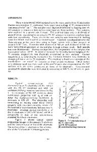
ABSTRACT Co(SiGe). contacts have been formed on low defect density, relaxed Si 01.Geo. 3 layers by conventional self-aligned contact processing techniques. Test structures measuring the contact metal sheet resistance indicate that the resistivity is high for anneal temperatures from 450'C to 750 0 C. The lowest sheet resistivity was 100 Q/O, about 10 times the resistivity of a comparable amount of CoSi 2 . Contact resistivities, measured by the transmission line method, were as low as 2 x 10⁻⁵ Q cm 2 . There is a large discrepancy between contact resistivities measured by transmission line and 4 point Kelvin test structures that may be due to the fabricated contact sizes.
INTRODUCTION Low resistance source/drain contacts to n-type SiGe alloys are necessary to exploit the improved transport properties of tensile strained Si on relaxed SiGe buffers in field effect transistors. The self-aligned silicide contact formation technique, using Ti or Co, can significantly reduce the contact resistance of conventional Si devices and should, in principle, be easily transferred to the SiGe material system. The metallurgical properties and resistivity of Co(SiGe). and CoGe 2 has been investigated by Ridgway [1] and Ashburn et al [2, 3]. However, the contact resistivity of Co(SiGe)> on n-type, implanted SiGe has not been reported. EXPERIMENTAL Test devices were fabricated on step-graded, relaxed, low defect density Si 0 7.Ge 0 .3 grown by rapid thermal chemical vapor deposition [4]. As+ was ion-implanted through a 10 nm screen oxide to convert the p- SiGe cap layer surface to n+. Structures were electrically isolated by forming a series of mesas through photolithography and reactive ion etching. A layer of Si0 2 was deposited and etched to form a series of windows exposing the SiGe beneath. Co was sputter deposited and the specimens were annealed in a vacuum at temperatures ranging from 400 to 7500 C to form Co(SiGe), only in the oxide windows. The unreacted Co was stripped by wet etching and Al contact pads were formed. More details will be published elsewhere [5]. Sheet resistance structures were formed on the un-implanted regions of the SiGe. They consisted of long bars, 10 and 20 pm wide. Current was driven from end to end along these bars and the voltage drops at various distances were measured. Contact resistivities were measured using two different test devices: the 4 point Kelvin structure and the transmission line method (TLM) structure [6]. Kelvin structure tests were performed by driving current through a semiconductor/silicide-germanide interface and measuring the voltage drop across the interface by way of a side tap in the semiconductor just next to the contact region. Devices were made with square contacts of 20, 30, 50 and 90jsm to a side. The contact resistivity, Pc, is equal to the product of the measured contact resistance, R,, and the contact area. 323 Mat. Res. Soc. Symp. Proc. Vol. 320. 01994 Materials Research Society
200 -
150
,'-c-:,-
uut3Iuejx
CL-
4.
areet
1:.-s .
-
Resiuonce
vs. Anneal Temp
Data Loading...


