The Origin of Electrical Activity at Grain Boundaries in Perovskites and Related Materials
- PDF / 520,812 Bytes
- 10 Pages / 612 x 792 pts (letter) Page_size
- 58 Downloads / 277 Views
The Origin of Electrical Activity at Grain Boundaries in Perovskites and Related Materials
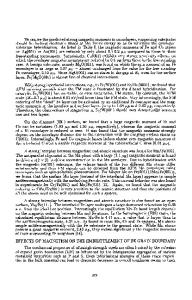
S. J. PENNYCOOKa,b, M. KIMa,c, G. DUSCHERa,b, N. D. BROWNINGc, K. SOHLBERGd and S. T. PANTELIDESa,b a Solid State Division, Oak Ridge National Laboratory, Oak Ridge, Tennessee 37831-6030 b Department of Physics and Astronomy, Vanderbilt University, Nashville TN 37235 c Department of Physics, University of Illinois at Chicago, Chicago, IL 60607-7059 d Department of Department of Chemistry, Drexel University, 3141 Chestnut Street, Philadelphia, PA 19104 INTRODUCTION In the last few years, the combination of atomic-resolution Z-contrast microscopy, electron energy loss spectroscopy and first-principles theory has proved to be a powerful means for structure property correlations in complex materials1. Here we demonstrate the effectiveness of this combined approach by demonstrating the origins of electrical activity at grain boundaries in the prototypical perovskite SrTiO3 and the high-temperature superconductor YBa2Cu3O7-x, materials that are closely related in structure. We show, both experimentally and theoretically, that grain boundaries in SrTiO3 are intrinsically non-stoichiometric. Electron energy-loss spectroscopy (EELS) provides direct evidence of non-stoichiometry, in agreement with totalenergy calculations that predict non-stoichiometric grain boundaries to be energetically favorable. The predicted structures are consistent with atomic-resolution Z-contrast Objective Lens micrographs. These results provide a consistent Forms a 1.3Å explanation of the grain boundary charge that was Probe previously inferred from electrical measurements, and provides a microscopic explanation of the GaAs resulting “double-Schottky barriers”. We also Z=31 Z=33 present experimental evidence for nonstoichiometry at grain boundaries in the hightemperature superconductor YBa2Cu3O7-x, where the same phenomenon explains the observed exponential reduction of critical currents with Annular Detector grain boundary misorientation. Our key experimental probe of grain boundary I ∝ Z2 atomic and electronic structure is the scanning Ga As transmission electron microscope (STEM). Such 1.4Å microscopes are now routinely available with EELS atomic-sized electron beams2, allowing atomic Spectrometer resolution Z-contrast imaging and EELS to be performed at the same time, as shown in the schematic of Fig. 1. The VG Microscopes Fig. 1. Schematic showing simultaneous HB603U STEM at ORNL has a 300 kV Z-contrast imaging and EELS in the accelerating voltage, with a directly interpretable STEM. The image distinguishes the resolution of 1.26 Å, and information transfer sublattice polarity in GaAs. AA1.3.1
demonstrated to 0.78 Å in Si〈110〉3, The Z-contrast image4,5 provides a direct image of atomic arrangements both at isolated dislocation cores6,7 and at dislocation arrays that comprise grain boundaries.8,9,10,11 The STEM probe can be located on an individual atomic column selected from the image for EELS measurements of local concentration and electronic structu
Data Loading...