Theoretical and Experimental Investigation of Disordering Effects on Photoluminescence Spectra of InGaAs/InGaAsP Quantum
- PDF / 1,419,594 Bytes
- 6 Pages / 414 x 635.4 pts Page_size
- 44 Downloads / 323 Views
ABSTRACT The effect of disordering on photoluminescence spectra of InGaAs/InGaAsP quantum wells has been investigated experimentally and theoretically taking into account the valence band intermixing, strain, exciton effects, and the non-identical diffusion constants for group III and V materials. The disordering profile of 1.55Q InGaAs/InGaAsP quantum wells lattice matched to InP has been controlled by choice of the cap layer materials as well as the diffusion time and diffusion temperature. By comparing the experimental data and theoretical calculations, the diffusion constant for each material has been extracted.
INTRODUCTION Quantum Well Disordering (QWD) has drawn a considerable attention in recent years[l-3] due to its wide applicability in the fabrication of optoelectronic devices. QWD allows modification of the shape of QW in the selected regions. Thus it modifies the subband energies in the conduction and valance bands[4]. This leads to the changes in optical properties such as band gap, absorption coefficient and refractive index. Hence such selected area disordering enables monolithic integration of various optoelectronic, such as lasers, modulators, waveguides and amplifiers. In this paper, we investigate the quantum well disordering effects on photoluminescence spectra by using experimental measurements and theoretical analysis. [5]
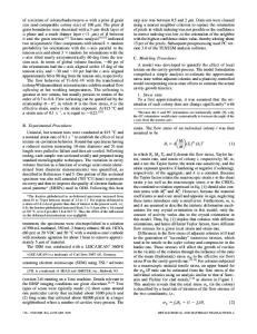
EXPERIMENT The disordering profile of 1.55Q InGaAs/InGaAsP quantum wells lattice matched to InP was controlled by the choice of the cap layer materials as well as the diffusion time and diffusion temperature. The cap layer materials chosen were InP, InGaAs, and InGaAsP with silicon nitride or silicon dioxide on them, respectively. The diffusion temperature was 750 'C and the diffusion time was varied up to 16 min. The largest PL peak shift observed was 120 meV when the cap layer was InP under silicon nitride. Figure 1 shows the actual epilayer structure (left) and the PL spectra measured at the room temperature(right).
519 Mat. Res. Soc. Symp. Proc. Vol. 607 © 2000 Materials Research Society
InP
50o
I
t4
....... ............. ........ . ........ .... ... . ...... . .
,
t--161
n-InP:Si 5e7l1W' n-InP
10 oo
---
substrate 1.3
1.5
1.4
1.6
Wavelength (pm)
Figure 1. Epilayer structure(left) and the PL spectra measured at the room temperature(right). The indicated times represent the diffusion time in minute.
ANALYSIS The disordering process in InGaAsfInGaAsP studied here is more complicated than the disordering of lattice matched InGaAs/GaAs or AlGaAs/GaAs QW structures. Disordering in the latter case is only due to the interdiffusion of group III (In, Ga) atoms, whereas interdiffusion in the present case can occur for both group III and group V (As, P) atoms. The structure consists of an Ino. 53Gao.47As layer sandwiched between thick Ino. 76Gao.24 Aso.51Po.49 barriers. After the disordering the concentration of the interdiffused atoms across the QW structure is assumed to have an error function distribution. The compositional profiles are represented as follo
Data Loading...