Thermal Activation of Beryllium in GaN Grown by RF-Plasma Molecular Beam Epitaxy
- PDF / 431,730 Bytes
- 6 Pages / 612 x 792 pts (letter) Page_size
- 64 Downloads / 311 Views
Y10.59.1
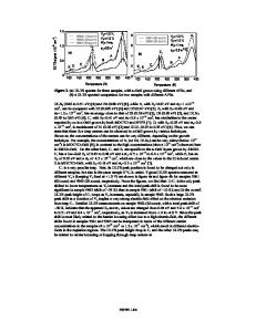
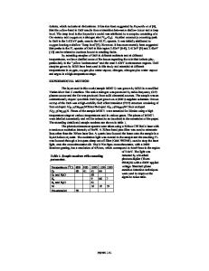
Thermal Activation of Beryllium in GaN Grown by RF-Plasma Molecular Beam Epitaxy B.L. VanMil, Kyoungnae Lee, Lijun Wang, N.C. Giles and T.H. Myers Department of Physics, West Virginia University, Morgantown, WV 26506 ABSTRACT Differences in the optical activity of Be in GaN epilayers grown on different surface polarities by rf-plasma molecular beam epitaxy are investigated. Nitrogen-polar GaN doped with Be exhibits a significantly higher intensity of donor-acceptor pair (DAP) photoluminescence (PL) than similarly doped Ga-polar GaN, indicating the Be is incorporating at microscopically different sites, or possibly is forming different compensating complexes. Highly Be-doped Ga-polar GaN apparently forms isolated polarity-inverted regions which then incorporate Be via the N-polar mechanism resulting in the DAP PL. High temperature annealing of the Ga-polar layers both under nitrogen/hydrogen mixtures and under pure nitrogen atmospheres activates the DAP PL. INTRODUCTION Beryllium remains a potential alternative p-type dopant for GaN. Several studies suggest that the activation energy for Be can be significantly lower than that of Mg. The strongest support comes from the interpretation of certain PL features as being related to DAP transitions, implying an optical activation energy of ~100 meV.1,2 There have been limited and difficult to reproduce reports of p-type conductivity for Be-doped GaN in oxygen contaminated cubic GaN3 and Be-implanted and annealed GaN.4,5 These studies had activation energies ranging from 127 to 231 meV. Unfortunately, no optical measurements were reported for the p-type layers and so direct comparison of PL features and activation energy can not be ascertained. To the best of our knowledge, there have not been any reports of as-grown wurtzite GaN doped with Be exhibiting significant p-type conductivity. In this study, we examine the growth surface polaritydependence of the optical activity of Be in GaN, and attempt to activate the Be using an anneal schedule similar to that used in ion implantation studies. EXPERIMENTAL Uniform and step-doped GaN layers were grown by rf plasma-assisted MBE using an EPI Unibulb nitrogen plasma source. A conventional effusion cell was used for Ga, and Be was evaporated from a dopant effusion cell (EPI-5-D). N-polarity GaN was obtained by nucleating GaN buffer layers directly on sapphire under heavily Ga-rich conditions. Ga-polar GaN was grown on MOCVD GaN templates on (0001) sapphire substrates. Uniformly Be-doped films of 1.0 µm thickness were grown on ~0.1 µm of undoped GaN. The doped layers were grown at a rate of 0.25 µm/hr, which corresponded to a nitrogen flow rate of 0.85 sccm and rf power of 200 W. The samples were grown under Ga-stable conditions (Ga/N flux ratio >1) which results in high quality GaN growth.6,7,8 Step-doped structures were produced by opening and closing the dopant shutter. In-situ growth rates were monitored using laser interferometry. All changes in oven and substrate temperatures occurred with the dopant shutter closed.
Data Loading...