Modulation of Arsenic Incorporation in GaN Layers Grown by Molecular Beam Epitaxy
- PDF / 506,062 Bytes
- 6 Pages / 612 x 792 pts (letter) Page_size
- 19 Downloads / 311 Views
Y8.4.1
Modulation of Arsenic Incorporation in GaN Layers Grown by Molecular Beam Epitaxy S.V. Novikov1,2, L.X. Zhao1, C.T. Foxon1, B.Ja. Ber2, A.P. Kovarsky2, I. Harrison3, M.W. Fay4 and P.D. Brown4 1 School of Physics and Astronomy, University of Nottingham, Nottingham, NG7 2RD, UK 2 Ioffe Physical-Technical Institute, St. Petersburg, 194021, Russia 3 School of Electrical and Electronic Engineering, University of Nottingham, Nottingham, NG7 2RD, UK 4 School of Mechanical, Materials, Manufacturing Engineering and Management, University of Nottingham, Nottingham, NG7 2RD, UK
ABSTRACT
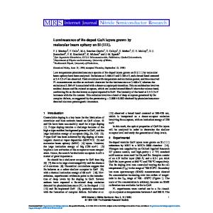
GaN layers periodically-doped with arsenic were grown by plasma-assisted molecular beam epitaxy on sapphire substrates. Secondary ion mass spectroscopy studies using different secondary ions clearly confirmed the existence of As-modulation in the GaN/GaN:As periodically-doped structures, however, the degree of As-modulation is still under discussion. The use of modulation doping with As has a strong influence on the optical properties of GaN/GaN:As structures.
INTRODUCTION
During the last few years there has been considerable experimental and theoretical interest in As-doped GaN [1-3, 4 and references therein]. There are three main reasons, which motivate such investigations i.e. an abrupt negative bowing in the energy band gap for GaNAs solid solutions, arsenic-stimulated growth of cubic phase GaN and strong blue emission at room temperature from arsenic doped GaN. Strong blue emission has been observed at room temperature for As-doped GaN films prepared by ion implantation, metal-organic vapour phase epitaxy (MOVPE) and plasmaassisted molecular beam epitaxy (PA-MBE) [1-4]. However, the mechanism responsible for the blue emission has not been definitively identified. There is some theoretical and experimental evidence to suggest that the blue emission is caused by recombination involving an arsenic antisite deep level defect (AsGa) [4,5]. Arsenic doped GaN films grown by PA-MBE on sapphire substrates show very strong blue emission at room temperature [4], which is more than one order of magnitude stronger than the band edge emission in undoped GaN films. Our results demonstrate that the growth conditions have a strong influence on the intensity of the blue emission from As-doped GaN grown by PAMBE [4]. For a fixed growth temperature and constant Ga and N fluxes, the intensity of the blue emission increases with increasing arsenic flux. For a fixed growth temperature and As flux the intensity of this blue emission increases for samples grown with an increased Ga:N ratio. For fixed Ga, N and As fluxes there is an optimum growth temperature of ~780oC at which the
Y8.4.2
highest blue emission intensity is observed. The As incorporation in our GaN layers was analysed using secondary ion mass spectroscopy (SIMS) [4]; using GaAs+ secondary ions, the As concentration was estimated to be between 1018 and 1019 cm-3 depending on the As flux. At the same time, Auger electron spectroscopy (AES) studies of the As-doped layers showed the exist
Data Loading...