Thickness Dependence and Electrical Properties of Ultrathin PZT Films Grown on SrRuO 3 /SrTiO 3 by MOCVD
- PDF / 694,013 Bytes
- 6 Pages / 417.6 x 639 pts Page_size
- 86 Downloads / 339 Views
Mat. Res. Soc. Symp. Proc. Vol. 596 © 2000 Materials Research Society
Surface morphology was observed using a field emission scanning microscope (FE-SEM) (Hitachi S-900) and scanning probe microscopy (SPM) (Seiko Instru. Inc. SP13800N). I-V characteristics and ferroelectric properties were measured using an electrometer (Keithley 6517), an LCR meter (HP 4262A), a Sawyer-Tower circuit, a pulse generator (HP 811OA) and a digitizing oscilloscope (HP 54616B). RESULTS AND DISCUSSION Thickness Dependence of Crystalline Structure SRO(001) films were epitaxially grown on a STO(001) substrate at a growth temperature of 530TC by rf magnetron sputtering. PZT(001) films were also successfully grown on SRO/STO at 580TC by MOCVD. X-ray rocking curve measurements and in-plane glancing incident X-ray diffraction measurements showed that PZT thin films obtained were epitaxially grown on a SRO(00 1)/
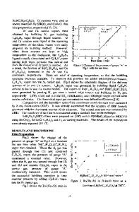
STO(001) substrate [9,10]. Polycrystalline SRO(110) orientated films were grown on Si0 2/Si at 580TC. Polycrystalline PZT films with (100) and (I10) mixed orientations were grown on SRO/ SiO2/Si [9,10]. Dependence of the lattice constant of the epitaxial PZT films on film thickness over the range of 40 to 400nm is shown in Fig. 1. The a-axis decreased and the c-axis increased as film thickness decreased. This result showed the same behavior in BaTiO 3/Pt/MgO [11,12]. PZT films obtained in our experiments showed tetragonal structures even when film thickness was less than 50nm. Figure 2 shows the dependence of the lattice constant of PZT, SRO and STO on temperature. This temperature dependence was measured using high temperature X-ray diffraction. The c-axis lattice constant of the PZT film decreased as temperature rose to 380 0C, and afterward was constant up to a temperature of 600TC. This indicates that the obtained PZT film had a phase transition temperature of 380TC. The difference in phase transition temperature between thin film and bulk PZT can be explained by the stress induced by the substrate [11,12]. Surface morphology of epitaxial PZT films was observed with FE-SEM as shown in Fig.3. SEM images revealed that the 40nm-thick and 400nm-thick PZT films showed smooth surface compared with that of polycrystalline PZT film on SRO/Si0 2/Si. No grain was observed for these epitaxial films.
0.420
.
, .
i
,
c-axis
E 0.415 cn 0 (1) 00
A2 0.410-
a-axis 0.4051
200
0
400
Film thickness (nm) Fig. 1 Dependence of lattice constant on the film thickness of epitaxial films.
260
&7
Pb(ZrTri)o 3 41
SrRuO 3
"C 8 0.
Srio 3
. o0. 39
E--'PZT 40nm
nt
0
400
200
600
Temperature (°C) Fig.2 Dependence of c-axis lattice constant of epitaxial PZT film on temperature. (a)
(b)
Fig.3 SEM images of epitaxial PZT thin films with a thickness of(a) 40nm and (b) 400nm. Thiekneiss Denendenee of Electrical Pronerties Thc ...........
n
s
of
Electrical....
..
ro
......
Thickness dependence of relative dielectric constant for epitaxial PZT films was measured. Figure 4 shows the reciprocal capacitance versus the film thickness for
Data Loading...