Epitaxial Growth of Titanium Nitride Films on (100) Silicon Three-Dimensional Heterostructures: Processing and Character
- PDF / 3,057,262 Bytes
- 6 Pages / 414.72 x 648 pts Page_size
- 85 Downloads / 409 Views
*Zycon Corporotion, 445 El Camino Real, Santa Clara, CA 95050. ABSTRACT
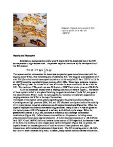
We have shown that epitaxial films can be grown on highly lattice mismatch systems by domain epitaxial growth. For titanium nitride films on (100) silicon substrates, it is shown that epitaxial growth can occur by matching m aTiN = n asi, where m and n are simple integers with values of 4 and 3 respectively, giving rise to less than 4.0% misfit. We have investigated the formation of epitaxial titanium nitride films grown on (100)Si by pulsed laser (KrF: ) = 248 nm, 'r= 25 ns) physical vapor deposition technique at different substrate temperatures, ranging from 200'C to 6001C. After optimizing the deposition conditions for epitaxial TiN film on Si, we have grown epitaxial silicon film on TiN. The epitaxial relationship was found to be Si II TiN II Si. This semiconductor-metal-semiconductor device configuration has potential applications in three-dimensional integrated circuits and radiation hardened devices. The success of this technology is predicted on our understanding of: (a) defects at interfaces of Si/TiN/Si, and (b) stresses/strains at interfaces. This paper focuses on the nature of epitaxial growth and analyzes the atomic structures of defects at Si/TiN/Si interfaces using high resolution transmission electron microscopy (HRTEM). These results are correlated with the results from theoretical modeling of Si/TiN/Si heterostructures. INTRODUCTION
Silicon-on-conductor (SOC) device configurations have currently been investigated [1, 2] as potential materials systems for radiation hardened devices and for three-dimensional integration of advanced semiconductor devices. Epitaxial TiN is a promising material for use as a conductor in metal-base transistors and as interconnects in 3-D integrated circuits. TiN has several advantages: high thermal and mechanical stability, diffusion barrier characteristics, good etch-stop capability etc. Laser ablation is one of the most desirable low-temperature processing techniques to grow single crystal epitaxial Si and TiN films. We recently reported [3, 4] the formation of Si/TiN/Si heterostructures by laser physical vapor deposition (LPVD), where it was shown that 4 unit cells of TiN match with 3 unit cells of silicon within 4% misfit with Si IITiN IISi epitaxial relationship. Domain epitaxial growth [5, 6] has become possible in this large mismatch system. We have calculated [3] the energy associated with the epilayer in the Si/TiN/Si structure and found that it is minimized via domain epitaxial growth. In this paper we establish an optimum condition for epitaxial growth of TiN films on Si(100) by using several characterization techniques, e.g. high resolution TEM, auger electron spectroscopy, and four-point probe sheet resistivity measurements. EXPERIMENTAL RESULTS
A pulsed KrF excimer laser ( X= 248 nm, and = 25 ns) was used to ablate titanium nitride from a stoichiometric hot pressed TiN pellet at a repetition rate of 5 Hz.2 The 2 cm-diam laser beam was focussed onto the target to obtain an energy den
Data Loading...