Ultra-Fast Melting and Solidification Behaviour of Amorphous and Crystalline Silicon
- PDF / 2,448,263 Bytes
- 6 Pages / 417.6 x 639 pts Page_size
- 83 Downloads / 239 Views
ULTRA-FAST MELTING AND SOLIDIFICATION BEHAVIOUR OF AMORPHOUS AND CRYSTALLINE SILICON A.G. CULLIS, H.C. WEBBER AND N.G. CHEW Royal Signals and Radar Establishment, Malvern, Worcs. WR14 3PS, England ABSTRACT Subnanosecond ultra-violet radiation pulses are used to produce relatively thick, large area amorphous layers on Si crystals by transient melting and solidification. The different behaviours of (001) and (111) Si orientations are highlighted. Observations of crystal growth phenomena during solidification at velocities lower than required for amorphization are correlated with theoretical predictions. Computer modelling of heat flow in amorphous silicon is refined. INTRODUCTION Q-switched laser annealing techniques provide a unique capability for the controllable exploration of fast melting, solidification and crystal growth processes in semiconductors. The present work focuses on three areas of current interest. By use of the highest quench rates it is possible to induce solidification of transiently molten crystal at such high speed that the lattice cannot reform and an amorphous solid is produced. Very short (O.7ns) pulses of ultra-violet radiation are used to produce particularly thick amorphous layers in Si by this method. For quench rates at which crystal can reform from the melt, it is found that regrowth characteristics are markedly orientation dependent with large differences between (001) and (111) surfaces. For much of the experimental work it is most important that computer modelling be used to ensure that the transient behaviour of the material is well understood. However, it has not previously been possible to quantitatively account for heat flow in amorphous semiconductors, although the approach described below yields a significant improvement in this situation. EXPERIMENTAL The samples used in these experiments were (001) or (111) Si crystals with surface layers that were either as-grown and defect-free or rendered amorqhous ýo a depth of llOO1 by implantation of 80keV As+ ions at a dose of 5xlO /cm . The surfaces of these samples were transiently melted with 1-3mm diameter, spatially uniform short radiation pulses taken from a Q-switched and pulse-chopped ruby laser system. Pulse lengths were either 0.7 or 2.5ns and radiation wavelengths were either 694 or 347nm. Annealed material was analyzed primarily by study of cross-sectional specimens in the transmission electron microscope (TEM). AMORPHIZATION PHENOMENA Previous studies of Si amorphization phenomena have employed radiation pulses of either tens of picoseconds or several nanoseconds duration [1- 3]. For a constant radiation wavelength, while the quench rate attained increases with decreasing pulse length the energy density threshold for surface damage Mat. Res. Soc. Syrup. Proc. Vol. 23 (1984) Published by Elsevier Science Publishing Co.,
Inc.
106
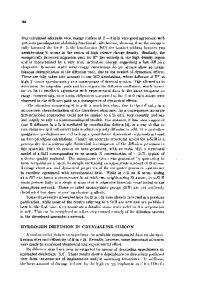
2.5ns
Si layers irradiated with FIG. 1. Cross-sectional TEM images of (001) 2 ; 0.7ns: (b) and (c) just 2.5ns: (a) O.3J/cm ultra-violet pulses. 2 below and above threshold near 0.5J/cm , respec
Data Loading...