Uniformity and Performance Characterization of GaN P-I-N Photodetectors Fabricated From 3-Inch Epitaxy
- PDF / 855,361 Bytes
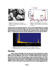
- 6 Pages / 417.6 x 639 pts Page_size
- 88 Downloads / 224 Views
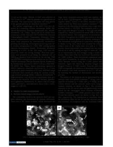
with unintentional n-type doping in the 1015 cm- 3 decade. The topmost epitaxial layer consisted of 2000 A 1.1018 cm-3 p-GaN. Mesas reaching the n-GaN cathode contact layer were formed by inductively coupled plasma (ICP) plasma etching with chlorine-based chemistry. Ohmic contacts to the n-type and p-type GaN were made by Ti-based and Ni-based metallizations, respectively. All of the GaN p-i-n UV detectors were fabricated with an optical detection area of 0.5 mm 2 and a p-i-n junction area of 0.59 mm 2, which is considerably larger (>12.5 times) than other GaN p-n detectors reported with noise measurements [1-3]. Shunt resistance and spectral responsivity data were collected using on-wafer probing. The shunt resistance was determined by the linear trace of the current-voltage (IV) characteristic from -10 mV to +10 mV. The spectral responsivities of the UV photodiodes were measured in photovoltaic mode (zero bias) using a 75 W xenon arc lamp chopped at 700 Hz and filtered by a 1/8 meter monochromator set to a 5 nm bandpass. The power of the monochromatic light was measured with a calibrated, NIST traceable, silicon photodiode and then focused onto the 3" GaN wafers resting on a micropositioner stage. The GaN p-i-n diode photocurrent was amplified, and the power spectral density in a 1 Hz bandwidth at the modulation frequency was monitored with a FFIT spectrum analyzer. Measurements of incident power and photodiode current were made in 10 nm intervals. For high temperature testing, individual GaN p-i-n photodiodes chips were diced from the wafers and mounted on a heated stage. All measurements were performed in an oxidizing, open air environment. The temperature dependent spectral responsivities were performed as described above. The 1/f noise measurements were performed with both the dice and heated stage mounted in an enclosure designed to suppress electromagnetic interference. For Il/f measurement, the signal from a battery powered, transimpedance amplifier-photodiode circuit was input into the FFT. The operational amplifier in the circuit was specified with a 1 kHz input noise current of 0.16 fA/Hz 12 , and the minimum noise power density of the measurement setup was approximately 4- 10-24 A 2/Hz. RESULTS All GaN UV photodector responsivity measurements reported here were obtained with the devices operating in the unbiased, photovoltaic mode. Shown in Figure 1 is a 25°C spectral responsivity curve for a UV photodetector with 0.194 A/W peak responsivity and 4 orders of 100
limit ef•eioncy, Quantun 16,
0.194A/W peakresponse
_10°
1.
.
.
..
Wavelength(nm)
Fig. 1: Typical GaN p-i-n UV photodetector unbiased spectral response.
20
+Icy do
b1.2-
10-
r +107
Mean
.P*,
_- - -2-c 0.8-0
+la \ 20 O_
W
0
10
20
3
2
1
0
+ 20
3
30 40 50 607080 100
Percent Fig. 2: Variation plot of unbiased peak responsivity normalized with the mean value.
X Position (mm) Fig. 3: Mean normalized unbiased peak contour plot for UV responsivity photodetectors verses position on a 3-inch GaN p-i-n wafer.
magnitude visib
Data Loading...


