X-ray Photoemission Determination of the Surface Fermi Level Motion and Pinning on n-and p-GaN during the Formation of A
- PDF / 48,805 Bytes
- 6 Pages / 612 x 792 pts (letter) Page_size
- 58 Downloads / 236 Views
X-ray Photoemission Determination of the Surface Fermi Level Motion and Pinning on nand p-GaN during the Formation of Au, Ni, and Ti Metal Contacts Kimberly A. Rickert,1 Jong Kyu Kim,2 Jong-Lam Lee,2 Franz J. Himpsel,3 Arthur B. Ellis,1 and T. F. Kuech4 1
Department of Chemistry, University of Wisconsin-Madison, Madison, Wisconsin 53706 Department of Materials Science and Engineering, Pohang University of Science and Technology, Pohang, 790-784, Korea 3 Department of Physics, University of Wisconsin-Madison, Madison, Wisconsin 53706 4 Department of Chemical Engineering, University of Wisconsin-Madison, Madison, Wisconsin 53706 2
ABSTRACT Synchrotron radiation-based x-ray photoemission spectroscopy was used to study the Fermi level position within the band gap for thin metal overlayers of Au, Ni, and Ti on n-GaN and pGaN. The Fermi level position was determined with the measured Fermi edge of the metal on the sample in order to correct for the presence of non-equilibrium effects. There are two different behaviors observed for the three metals studied. For Au and Ti, the surface Fermi positions on n-GaN and p-GaN are roughly 0.5 eV apart within the band gap. For Ni, the n-GaN and p-GaN have a Schottky barrier that forms at the same place at the gap. INTRODUCTION The development of high quality GaN growth techniques opened many device applications. GaN has a direct band gap of 3.4 eV that leads to the possibility of shorter wavelength light emission than previously achieved with other III-V semiconductor materials. GaN is used for a variety of these optical applications, including, but not limited to, light emitting diodes (LEDs)[1] and laser diodes.[2] GaN can also be used for microwave and high-power devices.[3] The large band gap of GaN makes the formation of low resistance ohmic contacts more difficult than for many other III-V semiconductors. The formation of low resistance contacts to p-GaN has been particularly challenging. Due to the complexity of metallurgical contacts, there are many variables that must be optimized to design better contacts. Many process variables have been changed in the various approaches to contact formation to create low resistance ohmic contacts including: chemical surface treatments[4-8] and plasma cleanings,[9-11] varying the metal deposition technique (sputtering, electron beam, or thermal depositions),[12-14] contact annealing in a variety of ambients,[15,16] and use of bilayers[17-19] or multilayers[20-22] of various metals. Most studies have focused on the electronic properties of a single metal[11,14,23-25] on either n-GaN or p-GaN surfaces. Results from these studies are difficult to compare directly due to the differences in sample carrier concentration, surface preparation prior to deposition and the techniques used to characterize the electronic properties (current-voltage, capacitance-voltage, or internal photoemission). In this investigation, a systematic study comparing three metals on identically prepared samples was carried out, allowing a direct comparison of the surf
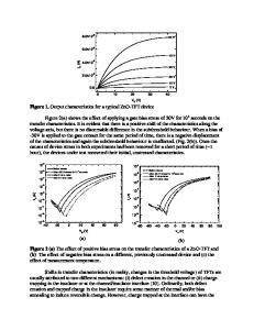
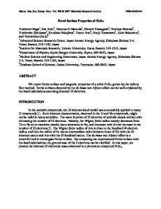
Data Loading...