A comparison of in situ As doping with ex situ CdCl 2 treatment of CdTe solar cells
- PDF / 1,840,380 Bytes
- 6 Pages / 612 x 792 pts (letter) Page_size
- 51 Downloads / 323 Views
F3.4.1
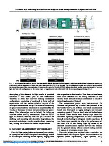
A comparison of in situ As doping with ex situ CdCl2 treatment of CdTe solar cells Vincent Barrioz1, Rachael L. Rowlands1, Eurig W. Jones1, Stuart J. C. Irvine1, Guillaume Zoppi2 and Ken Durose2 1 Department of Chemistry, University of Wales, Bangor, Gwynedd LL57 2UW, UK 2 Department of Physics, University of Durham, Science Laboratories, South Road, Durham DH1 3LE ABSTRACT A comparison has been made of MOCVD grown CdTe/ CdS solar cells processed either by ex situ annealing with CdCl2 or doping with arsenic, in situ, together with various optional anneals. A materials comparison was made of both routes using Jsc measurements on arrays of gold contacts to the CdTe. The Jsc increased from around 1 mA cm-2 for undoped and unannealed layers to a range of 25-30 mA cm-2 for CdCl2 annealed layers. In situ arsenic doping resulted in Jsc values up to 18 mA cm-2. The annealing characteristics were very different for these films, compared with the CdCl2 annealed films, with annealing at 500o C dramatically reducing the Jsc. Only annealing under nitrogen at 400o C produced an improvement in Jsc and further evidence from SIMS analysis suggests that hydrogen passivation of the arsenic dopant may have a significant effect on the dopant activity. INTRODUCTION Thin film structures of CdTe and CdS have been grown onto ITO coated glass substrates using Metal Organic Chemical Vapour Deposition (MOCVD) [1-3]. This method of deposition allows for a high degree of control over the material properties and very low background impurity concentrations. It is an ideal technique to study the phenomenology of CdTe/CdS solar cells, with the ability to dope with different impurities and control the deposition temperature over a range from 300o C to 500o C. The more commonly used Close Space Sublimation (CSS) process has been used to achieve record cells (16.5% AM 1.5 efficiency) [4] but as the technique uses relatively high temperatures followed by a subsequent anneal with a coating of CdCl2, it is not easy to understand the variety of material processes that can contribute positively (or negatively) to the efficiency of the cell. This paper reports on an on-going study using MOCVD to obtain a better understanding of the material processes and to establish a path to improved efficiency and device stability. In the past MOCVD has been shown to be suitable in providing thin films of CdTe on Chemical Bath Deposited (CBD) CdS that are then made into photovoltaic devices by a cadmium chloride treatment and annealed [1, 5]. In common with other techniques for depositing CdTe, the photoresponse is low prior to the anneal treatment. This paper reports on a comparison of the more conventional CdCl2 treatment of the MOCVD deposited layers with the in situ arsenic doping, with no ex situ treatment. By this means it is possible to benchmark the performance of the less conventional in situ doping and contrast the materials characterisation. EXPERIMENTAL All the CdTe and CdS layers used in this study were deposited by MOCVD [2] using the precursors dime
Data Loading...