A Current Conduction Mechanism in Laser Recrystallized Silicon Metal-Oxide-Semiconductor Transistors
- PDF / 415,100 Bytes
- 6 Pages / 420.48 x 639 pts Page_size
- 20 Downloads / 232 Views
A CURRENT CONDUCTION MECHANISM IN LASER RECRYSTALLIZED SEMICONDUCTOR TRANSISTORS
SILICON METAL-OXIDE-
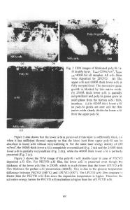
Han-Sheng Lee Electronics Department General Motors Research Laboratories Warren, Michigan 48090-9055 ABSTRACT N-channel MOS transistors were fabricated on silicon films that had been recrystallized by an argon ion laser at different power levels. These transistors showed electrical characteristics similar, but somewhat inferior to those devices fabricated on single crystal silicon substrates. These differences are attributed to the presence of trapping states at the grain boundaries of the crystallites in the recrystallized silicon. A coulombic scattering model is presented to explain these differences. In the case of films annealed at low laser power, an additional factor of nonuniform trap state distribution is invoked to explain device characteristics. This model provides an adequate explanation for the observed transport properties of transistors fabricated from recrystallized silicon films. INTRODUCTION Lasers have been used for annealing ion implantation damage and increasing the current handling capability and switching speed of thin-film transistors by enlarging the grain sizes of the deposited semiconductor substrates [1-7]. Even though considerable research has been done on the model of bulk current conduction in the polycrystalline silicon material, there are few reports on the surface current conduction mechanism [5-9]. The surface conduction mechanism is very important because it determines the current flow in MOS transistors. In polycrystalline silicon, the intercrystalline potential barrier, created by the carrier concentration difference between the crystallite and grain boundary region, plays a dominant role in the bulk conduction [10). In MOS transistors the intercrystalline potential barrier could be diminished by the increase of the applied gate voltage; however, the current handling capability is still less than those made with single crystal substrate material. We believe the coulombic scattering from trapped charges at the grain boundaries plays an important role in such a situation. In this report, we use the Rutherford scattering model proposed by Wu and Yang [11], the measured Id-Vd (drain-to-source current vs drain-to-source voltage) results from MOS transistors and the C-V (gate-to-substrate capacitance vs gate-to- substrate voltage) results from test capacitors to support our arguments. RESULTS The structure and the preparation details of the test transistors were described in Ref. [6]. Figure 1 shows the cross-sectional view of a finished transistor. The silicon film on which transistors were 1labrijated had a thickness of 0.65 pm and was implanted with boron to lxlO cm at 90 keV. The supporting material for this film was a single crystal silicon wafer. A scanning argon ion laser was used to recrystallize the polycrystalline silicon film with powers ranging from 10 to 15 W at 1 W increments. The gate oxide of the transistors was thermally grown at 1100%C with 3% HCI in dry oxygen am
Data Loading...