A Novel Method for the growth of Low Temperature Silicon Structures for 3-D Flash Memory Devices
- PDF / 168,282 Bytes
- 5 Pages / 595 x 842 pts (A4) Page_size
- 7 Downloads / 268 Views
1112-E05-03
A Novel Method for the growth of Low Temperature Silicon Structures for 3-D Flash Memory Devices Thomas A. Mih, Richard B. Cross and Shashi Paul1 Emerging Technologies Research Centre (EMTERC), Faculty of Technology, De Montfort University, LE1 9BH Leicester, United Kingdom.
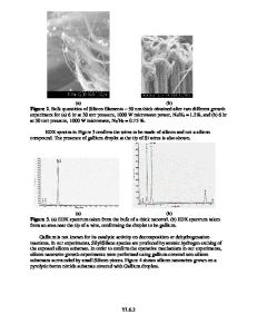
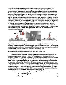
ABSTRACT Low temperature (≤400oC) growth of polycrystalline silicon (poly-Si) is carried out using plasma-enhanced chemical vapour deposition (PECVD). After an initial preparation step (IPS) poly-Si was grown on the substrates. Optical band gap studies of the poly-Si films have been correlated to the hydrogen content of the films, as well as to their photoconductivity. Furthermore, the suitability of these films for use as information storage materials for future generation 3-D flash memory devices is investigated using currentvoltage (I-V) and capacitance-voltage (C-V) measurements via metal-insulatorsemiconductor device structures. C-V analysis indicates strong charge storage behaviour for the poly-Si films. 1.0 INTRODUCTION Memory devices play a vital role in consumer electronic applications. Flash memory, a type of non-volatile memory ideal for portable applications such as mobile phones, digital cameras, laptop computers, has evolved over the years since its invention. Despite the enormous commercial success, current flash memory technology has some limitations for which a number of solutions are sought [1-4]. One such solution is three-dimensional (3-D) integrated logic [4], in which a number of memory layers are stacked on top of a silicon wafer using conventional CMOS technology. The flash memory industry widely employs chemical vapour deposition techniques to grow poly-Si, which is used as the information storage element. The growth temperatures of this technique are typically greater than 600oC. These high temperatures not only result in high thermal budgets in the fabrication of flash memory, but could also adversely affect device performance of next generation 3-D flash memory devices, where the need for high memory density and performance requires the substrates supporting the memory layers to be thinned down. Therefore, the development of low temperature processes is of fundamental importance to future 3-D integration. S. Paul has recently succeeded in growing poly-Si at temperatures ≤ 400oC using a PECVD technique, where the substrate underwent an IPS [5]. It is a low thermal budget method and is also CMOS compatible. The method described below is very different from the metal-induced crystallisation (MIC) and metal-induced lateral crystallisation (MILC) methods [6-8], in that the poly-Si is grown directly without having to first grow and then thermally anneal hydrogenated amorphous silicon (a-Si:H) films.
1
Corresponding author: Email: [email protected]
2.0 EXPERIMENT In this study, p-type silicon (1-10Ω, Boron doped) and glass substrates were used. To investigate the effect of the IPS, two sets of substrates were produced: those having undergone the IPS and those which had not. These were subsequently introduced
Data Loading...